A four-day PCB turnaround in Shenzhen or San Jose is a solved problem. You upload your Gerber and centroid files, pay forty dollars for air express, and have five populated boards on your bench by Thursday morning.
If your bench is in Riyadh, Dubai, or Cairo, that four-day turn routinely turns into sixteen days. The bare boards sit in an air cargo warehouse in Bahrain or Dubai World Central for seventy-two hours pending customs classification. Your component parcel from Mouser hits a clearance freeze because a microcontroller was flagged as encrypted radio equipment. By the time your DHL or FedEx courier rings your bell, your sprint timeline is dead, your investor update is delayed, and you are paying import handling fees that exceed the total BOM cost.
Building hardware in the GCC means accepting that you do not have a dense ecosystem of local quick-turn surface-mount assembly shops next door. You cannot drop off a reel of STM32s and a handful of cut tapes at a local contract manufacturer at 9:00 AM and pick up ten clean boards at 5:00 PM.
Survival as a solo hardware engineer or small deep-tech team in the region requires building your own logistics pipeline. You need to know when to pay for turnkey overseas assembly, when to build in-house with frameless stencils and a benchtop hot plate, and how to structure your BOM so your components do not rot in customs.
The GCC Customs Gauntlet: HS Codes and Compliance
The biggest delay in regional hardware prototyping is almost never the fab. Fabricators routinely etch, drill, plate, and assemble four-layer boards in 48 hours. The delay happens at port of entry.
Every shipment crossing into Saudi Arabia, the United Arab Emirates, or Egypt must clear regional regulatory frameworks. In Saudi Arabia, commercial imports route through ZATCA customs and frequently touch the Saber electronic platform. In the UAE, items pass through customs under the Federal Tax Authority and Ministry of Industry and Advanced Technology (MoIAT) oversight. In Egypt, shipments interface with the Advance Cargo Information (ACI) system via the Nafeza platform.
When a courier ships your PCB under a generic classification, customs agents inspect the parcel manually. A bare printed circuit board should strictly fall under HS Code 8534.00 (Printed circuits). Populated boards fall under HS Code 8542.31 or 8543.70 depending on the integrated circuit complexity and final functionality. If your supplier puts "electronic parts" or "computer board" on the commercial invoice, the package gets pulled aside.
HS CODE REFERENCE FOR PROTOTYPING:
------------------------------------------------------------
8534.00.00 : Bare Printed Circuit Boards (No components mounted)
8542.31.00 : Monolithic Integrated Circuits (Processors, MCUs)
8541.10.00 : Diodes (other than photosensitive or LEDs)
8532.24.00 : Multilayer Ceramic Capacitors (MLCCs)
8533.21.00 : Fixed Electrical Resistors (Power <= 20W)
8543.70.90 : Electrical Machines/Apparatus with unique functions (Assembled test boards)
For microcontrollers with integrated wireless radios (ESP32-S3, nRF52840, STM32WB55), customs officers in the GCC often request clearance from local communications authorities: CST in Saudi Arabia, TDRA in the UAE, or NTRA in Egypt. If you import a finished PCBA with an uncertified onboard radio module without commercial paperwork, customs can hold it indefinitely or demand formal type approval.
To prevent this on prototype runs, use pre-certified RF modules (such as u-blox NINA or Espressif modules with visible FCC/CE/telecom marking IDs) rather than chip-down RF designs for Revision 0. When shipping assembled prototypes, ensure your overseas manufacturer explicitly lists them as "Engineering Prototype Samples - For R&D Testing Only - Not for Commercial Resale" on the commercial invoice alongside the exact HS code.
Turnkey Overseas Assembly vs. The In-House Desk-Fab
Solo engineers face a binary choice on every revision: do you outsource the entire assembly to a turnkey fab house in China or Europe, or do you order bare boards, ship components from major distributors, and paste the boards yourself?
When Turnkey Assembly Fails in the Gulf
Turnkey assembly services (such as JLCPCB, PCBWay, or FastTurn PCB) are unmatched on price. Sourcing components through their in-house parts libraries eliminates distributor shipping costs and feeder setup charges. If you design entirely around their "basic" or "preferred" parts catalog, a batch of five fully assembled boards can cost less than $150.
However, the pipeline breaks down the moment your board requires a component outside their standard library. An extended component requires an automated feeder reel change, adding setup cost and two to three days of sourcing from local distributors. If a part is out of stock in China, shipping that single missing analog front-end from an American distributor into Shenzhen adds a week before board fabrication even starts.
Add five days of fabrication and assembly, followed by four to seven days of international transit and GCC customs clearance. Your turnaround time is now two to three weeks. If you made a layout error on a single footprint or reversed the TX/RX pair on an unexposed trace, that three-week wait must be repeated from scratch.
The Desk-Fab Alternative: SMT Stencil and Hot Plate
For Revision 0 and Revision 1, the fastest path to a working board in Riyadh or Dubai is often local benchtop assembly.
This workflow decouples bare board manufacturing from component acquisition:
- Bare boards: Order standard 4-layer FR4 with 1-day or 2-day turn from an overseas fab with DHL Express. Bare boards pass customs with minimal friction under HS 8534.00.
- Stencil: Order a stainless steel, frameless stencil (0.10mm or 0.12mm thickness) alongside the bare boards.
- BOM: Order the complete bill of materials from DigiKey, Mouser, or Farnell via express carrier.
Both parcels travel simultaneously and arrive within four to five working days. You then assemble two boards in two hours on your bench.
DESK-FAB SETUP FOR HIGH-DENSITY BOARDS:
- Hot Plate: Miniware MHP30 (for small sub-boards) or 200x200mm PTC heating plate
- Solder Paste: Sn42Bi57.6Ag0.4 (Low-temp, 138°C melt) or SAC305 (Standard, 217°C melt)
- Dispensing: 3D-printed stencil jig with manual squeegee (stainless blade)
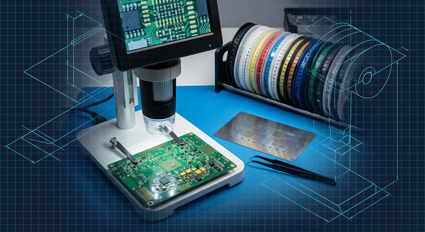
- Placement: Manual vacuum pick-and-place pen with foot switch, paired with a 20x stereo microscope
- Rework: Quick 861DW hot air rework station with angled nozzles
This strategy is particularly effective for packages down to 0.5mm pitch: QFNs, SOICs, TSSOPs, and 0402 passives. For fine-pitch packages and 0.4mm pitch CSPs or BGAs, manual paste alignment with a frameless stencil becomes challenging without a mechanical stencil printer frame.
If you must use BGAs on early prototypes, choose packages with a 0.8mm ball pitch where possible. At 0.8mm pitch, you can route escape tracks without blind or buried microvias, standard 0.1mm solder mask dam clearance holds up, and hand-placed alignment is achievable under a stereo microscope using optical tick marks on the top silkscreen.
Managing Solder Chemistry in High-Ambient Climates
One overlooked failure mode in Gulf hardware labs is solder paste degradation. When ambient workshop temperatures reach 28°C to 35°C during summer months or when air conditioning is cycled off overnight, standard solder paste undergoes rapid rheological changes.
Solder paste is a suspension of microscopic solder alloy spheres within a thixotropic flux carrier. Exposure to ambient heat accelerates flux volatilization and oxidation of the alloy spheres. If you leave a solder paste jar or syringe on your bench in an unconditioned room, the paste dries out within days.
When dry paste is forced through a 0.12mm stainless stencil, it causes bridging across 0.5mm QFN pins and voids beneath power pads because the flux burns off before the liquidus state is reached.
SOLDER PASTE HANDLING RULES:
- Storage: Keep paste containers refrigerated at 2°C to 8°C.
- Stabilization: Allow the syringe or tub to reach room temperature (20-22°C) naturally for 2 hours before opening. Opening cold paste causes atmospheric condensation inside the container, leading to solder spatter during reflow.
- Alloy Selection for Hot Plates: Sn42Bi58 or Sn42Bi57.6Ag0.4 melts at 138°C. This allows low-stress reflow on low-cost aluminum hot plates without blistering FR4 or melting nearby plastic connectors.
- Alloy Selection for Field Units: If the device will operate in harsh GCC outdoor conditions (solar, automotive, or industrial monitoring where ambient temperatures exceed 50°C), avoid low-temperature bismuth alloys. Use SAC305 (96.5% Sn, 3.0% Ag, 0.5% Cu) with a peak reflow temperature of 240°C to 245°C.
Component Sourcing: Local Markets vs. Direct Imports
Every regional hardware ecosystem has a local electronics market: Bab El-Louk in Cairo, the Deira electronics market in Dubai, or Batha in Riyadh. These shops are useful for basic maintenance, field wiring, and educational projects. You can find standard terminal blocks, 1N4007 diodes, NE555 timers, 1/4W through-hole resistors, and common soldering iron tips.
They are largely useless for commercial-grade fast-turn hardware engineering.
You will rarely find a high-efficiency synchronous buck regulator (such as a Texas Instruments TPS62840 in a tiny WCSP), a modern ultra-low-power Cortex-M33 MCU, or precision 0.1% 0402 resistors in local market stalls. Attempting to source critical semiconductor parts locally often exposes you to old component date codes, questionable storage conditions, or counterfeit ICs with ground-down packaging markings.
For professional prototype runs, stick to authorized global distributors (Mouser, DigiKey, Element14/Farnell). To minimize customs clearance delays and shipping overhead, use the following operational rules:
1. The Consolidation Window
Never order components piecemeal across three different distributors for a single revision. Each individual airway bill incurs its own administrative clearance charge (often $30 to $50 per parcel regardless of product value) from the courier. Consolidate your entire BOM into a single order with one vendor. If one specialized part is exclusive to another platform, find a drop-in second source or adjust the schematic before placing the order.
2. DDP (Delivered Duty Paid) Shipping Terms
Always select DDP at checkout where available (DigiKey and Mouser support this for most GCC destinations). With DDP, the distributor calculates the VAT and customs duty at the point of sale and acts as the importer of record with the courier. Parcels shipped under DDP terms glide through regional customs hubs because the clearance fees are settled automatically on the corporate account, bypassing the manual payment collection queue.
3. Maintain a Local "Jellybean" Lab Stock
Solo engineers cannot afford to order passive components every time a pull-up resistor or filtering capacitor changes. Keep a stocked library of 0402 and 0603 passive sample books on your lab shelf:
- Resistors: 1% 0402 and 0603 series from 0 ohms to 1M ohms.
- Ceramic Capacitors: 50V X7R 0402/0603 assortments (1pF through 10uF).
- Inductors: Common power inductor values (1.0uH, 2.2uH, 4.7uH, 10uH) in standard 2016 and 3030 metric sizes.
- Diodes and Transistors: Common dual N-channel and P-channel MOSFETs (such as 2N7002, BSS138), Schottky diodes (BAT54 series), and TVS electrostatic protection diodes.
- Connectors: JST-SH (1.0mm pitch), JST-PH (2.0mm pitch), standard 1.27mm and 2.54mm pin headers, and USB-C 16-pin mid-mount receptacles.
With these basic parts on hand, you only need to import the core semiconductors, power management ICs, and bare boards for each iteration.
Layout and DFM Rules for First-Pass Gulf Prototyping
When your respin turnaround is two weeks instead of three days, your design-for-manufacturing (DFM) discipline must be airtight. Every DRC failure or unrouted trace caught on the bench represents dead time.
Generous Footprints and Probe Access
When laying out Revision 0, do not optimize for minimum form factor unless your mechanical enclosure strictly dictates it.
Use expanded footprint pads (IPC-7351 Level A - Maximum land protrusion) rather than nominal or density-optimized pads. Adding 0.2mm of copper length to the toe of a QFN pad allows hot air rework tweezers or a micro-soldering iron tip to reach the joint directly without relying entirely on convection under the package.
Place test points on every power rail, reset pin, SPI bus, I2C line, and UART interface. Make them large enough for micro-gripper hooks (minimum 1.0mm diameter copper pad with 0.8mm solder mask opening), and keep them on the top layer. If an internal sub-circuit fails to start up, cutting a trace with a scalpel and soldering a 30 AWG kynar jumper wire is trivial if test pads are readily accessible.
REVISION 0 PCB LAYOUT CHECKLIST:
[ ] 1.0mm test pads on 3V3, 5V, VBUS, Battery, and all internal buck rails
[ ] Dedicated ground test loop for oscilloscope spring-ground clips
[ ] Hardware-isolated 0-ohm resistors on all functional power domain inputs
[ ] UART TX/RX broken out to standard 2.54mm header pads for early boot logging
[ ] Thermal reliefs enabled on all ground plane connections (0.25mm spoke width)
[ ] Clear pin 1 indicators on silkscreen and copper layers outside package boundary
[ ] Pull-up resistors on open-drain lines (I2C, Reset) explicitly placed, not assumed internal
Thermal Reliefs for Manual Rework
Solid copper plane connections to SMD passive pads provide excellent electrical and thermal performance, but they make manual soldering painful. An unheated copper ground plane sinks heat away from an iron tip instantly, leading to cold solder joints or ripped copper pads during rework.
Always enforce 4-spoke thermal reliefs on all plane connections for prototype revisions. Set your spoke width to 0.25mm or 0.3mm with a 0.25mm air gap. This preserves adequate current capacity while enabling clean soldering using a standard 65W soldering iron at 350°C.
Modern layout tools and AI-assisted autorouting platforms like IntelCAD streamline this process by automating design-rule checks and thermal relief generation according to local fab capabilities, preventing simple layout oversights before Gerber export.
The 7-Day Gulf Prototyping Cycle
Below is the battle-tested timeline used by hardware startups in the region to move from schematic freeze to functional firmware testing on physical hardware within seven working days:
| Day | Phase | Action Items |
|---|---|---|
| Day 1 (Mon) | DRC & Freeze | Complete schematic capture. Run DRC checks on 4-layer stackup. Audit BOM against distributor stock (DigiKey/Mouser). Export Gerbers, drill files, centroid, and BOM. |
| Day 2 (Tue) | Procurement | Order bare boards + frameless stencil from fab house via Priority Express. Order consolidated BOM from distributor using DDP terms. Verify commercial invoices show exact HS codes. |
| Day 3 (Wed) | Firmware Prep | Write low-level board support package (BSP), register maps, and peripheral drivers against MCU vendor HAL or register-level emulation while parts are in flight. |
| Day 4 (Thu) | Customs Tracking | Monitor courier tracking. If airway bill flags customs inspection, submit commercial invoice and prototype non-commercial declaration immediately via the carrier portal. |
| Day 5 (Fri) | Delivery | Receive board and component packages. Verify bare board impedance, check for shorts between internal plane layers using a digital multimeter before mounting components. |
| Day 6 (Sat) | Assembly | Apply solder paste through frameless stencil onto bare PCB. Place components under stereo microscope. Reflow via hot plate or benchtop convection oven. Inspect all QFN/IC pins. |
| Day 7 (Sun) | Bring-up | Power-on sequence using current-limited bench supply (limit to 50mA). Verify core rail voltages. Flash bootloader and blink test LED over SWD/JTAG debugger. |
Summary of Key Actions
To move fast without a domestic assembly infrastructure, treat logistics with the same engineering rigor you apply to high-speed differential routing. Consolidate your component supply chain around distributors that handle regional DDP clearance cleanly. Master benchtop low-temperature paste reflow with frameless stencils so you are never blocked by overseas extended feeder delays on early iterations.
Keep high-density 0402 passives, basic silicon switches, and test headers organized in your own lab. When you design your layout, expose test points, apply thermal reliefs to ground connections, and use pre-certified wireless modules on your initial runs. This keeps your prototype out of customs inspection queues and gets working silicon on your bench in days rather than weeks.
Sources
- Local PCB Sourcing for Faster Turnaround Times: https://www.vse.com/blog/local-pcb-sourcing-for-faster-turnaround-times/
- How to Get a Quickturn PCB Prototype in USA: https://www.protoexpress.com/blog/how-to-get-quickturn-pcb-prototype-usa/
- FastTurn PCB Assembly and Fine-Pitch Manufacturing: https://www.fastturnpcbs.com/
- MENA Integration into Global Value Chains: https://theforum.erf.org.eg/2025/09/15/mena-integration-into-global-value-chains-and-sustainable-development/