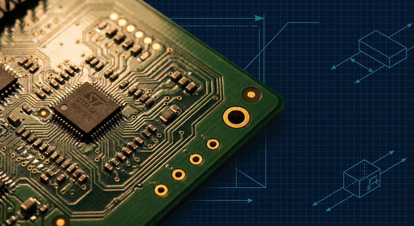
We took a completed, tested 4-layer mixed-signal board based on an STM32G474, stripped all the copper traces, and handed the unrouted netlist to Quilter and DeepPCB.
The board is a standard 50 x 50 mm four-layer stackup. It runs a 170 MHz Arm Cortex-M4 microcontroller, a switching buck converter stepping 12V down to 3.3V at 1.5A, a USB 2.0 Full Speed interface, two SPI sensor buses running at 20 MHz, and four channels of 12-bit analog input filtered through precision op-amps.
Every hardware engineer who has touched board layout in the last twenty years knows why autorouters have a terrible reputation. Old grid-based or topological autorouters from the Specctra era treated a PCB as a pure geometric graph search problem. They solved connectivity, but they destroyed signal integrity. They punched via fences straight across continuous ground planes, created massive loop areas on high-di/dt decoupling paths, ran single-ended noisy digital lines parallel to high-impedance analog signals, and left copper islands starved of return paths.
Over the last two years, machine learning and physics-informed layout tools have claimed to solve this. DeepPCB uses deep reinforcement learning to predict route paths based on trained board patterns. Quilter applies physics-driven simulations and reinforcement learning to place components, calculate return paths, and iterate board candidates through cloud compute.
We wanted to see what actually happens to return paths, decoupling loop inductance, and differential pairs when you strip human intuition out of the loop and give the netlist to modern algorithms.
The Test Board and Stackup Constraints
The test design uses a standard JLC04161H-7628 stackup on 1.6 mm FR-4, which is typical for low-cost fast-turn prototyping:
- Layer 1 (Top): High-speed signals, analog front-end, component placement.
- Layer 2 (Inner 1): Continuous Ground plane (0.5 oz copper, 0.21 mm prepreg below Layer 1).
- Layer 3 (Inner 2): Power rails (3.3V digital, 3.3V analog, 12V input) and non-critical low-speed routing (1.065 mm core below Layer 2).
- Layer 4 (Bottom): Secondary signal routing and ground fill.
In our manual KiCad baseline layout, all critical high-frequency return paths sit directly on Layer 2. The 0.21 mm dielectric thickness between Top and Inner 1 provides a tight loop with approximately 0.5 to 0.8 nH of parasitic inductance per via pair when decoupling 0402 ceramic capacitors directly to the microcontroller power pins.
For the automated tests, we fixed the component placement in the exact positions of our verified production layout for one run, and allowed the tools free placement for a second run. We exported the designs via standard IPC-D-356 netlists and Specctra DSN files, loaded the design rules into both engines, and let them route.
Here is how the automated tools handled the four critical layout challenges.
Decoupling Capacitor Loop Inductance
The STM32G474 has multiple VDD/VSS pin pairs. To keep transient supply rail ripple below 50 mV during clock edge transitions, each VDD pin requires a 100 nF 0402 ceramic capacitor located as close as possible to the pin, with direct via connections into Layer 2 ground and Layer 3 power.
The Manual KiCad Baseline
In our manual layout, the capacitor sits within 1.2 mm of the BGA/QFP pad. The VDD trace goes directly from the IC pad through the capacitor pad to the power via, or drops immediately into the plane. Ground vias sit right beside the capacitor ground pad, keeping the total round-trip loop inductance under 1.2 nH.
DeepPCB Results
DeepPCB completed 100% of the digital routes, but it treated decoupling capacitors as generic two-terminal nets to be solved whenever the geometric solver reached that area.
In three instances, DeepPCB routed the VDD trace from the MCU pin across 14 mm of top-layer copper before hitting the capacitor pad, while dropping a via to the 3.3V power plane directly under the MCU. This completely defeats the high-frequency bypassing function of the 0402 cap. The resulting parasitic trace inductance exceeded 8 nH. At 170 MHz switching speeds, that creates measurable ground bounce and supply sag on the internal core logic.
DeepPCB does not natively understand the concept of power delivery network (PDN) impedance hierarchy unless you manually lock the decoupling traces prior to initiating the cloud routing run.
Quilter Results
Quilter performed substantially better on PDN topology. Because Quilter integrates basic electromagnetic and thermal simulation models into its reinforcement learning reward function, it recognized that bypass capacitors must be kept physically and electrically tight to their parent power pins.
When we allowed Quilter to route the fixed placement, it dropped vias immediately adjacent to the 0402 capacitor pads and maintained short, wide copper necks (0.35 mm) between the MCU pins and the capacitor pads. Loop inductance averaged 1.6 nH across all MCU supply pins. It was not quite as tight as an experienced human laying out dog-bones by hand, but it was fully functional and avoided the disastrous long-trace bypass traps of older autorouters.
Ground Plane Integrity and Plane Slotting
The single biggest failure mode of traditional autorouters is plane perforation. When an autorouter drops twenty vias in a straight line to transition a bus between Top and Bottom, it slices the inner ground plane in half, creating a slot. Any high-speed trace crossing that slot experiences an immediate impedance discontinuity and radiates EMI.
We specifically looked at how both engines routed an 8-bit parallel digital bus and two 20 MHz SPI buses across the board.
Return Path Continuity Comparison (Inner Layer 1 Ground Plane)

+----------------------+--------------------+---------------------+-------------------+
| Metric               | Manual Layout      | Quilter Run         | DeepPCB Run       |
+----------------------+--------------------+---------------------+-------------------+
| Total Via Count      | 48                 | 62                  | 94                |
| Ground Plane Slots   | 0                  | 0                   | 3 minor slots     |
| Max Loop Area (SPI)  | 2.1 mm²            | 3.8 mm²             | 11.4 mm²          |
| Copper Balance (Top) | 42%                | 48%                 | 31%               |
+----------------------+--------------------+---------------------+-------------------+
DeepPCB
DeepPCB relied heavily on Layer 4 for escape routing, dropping signal vias indiscriminately through Inner Layer 1. Around the dense 64-pin microcontroller breakout, it clustered 18 vias with less than 0.2 mm clearance between drill holes.
This created a 6 mm unbroken void in the Inner Layer 1 ground plane. Two 20 MHz SPI clock lines on Layer 1 were routed directly over this void. In a bench test, crossing a 6 mm plane void on a 20 MHz clock with a 3 ns rise time would create substantial near-field radiation and ringing. DeepPCB solved the netlist, but the board would likely fail radiated emissions compliance at 200 to 400 MHz harmonics.
Quilter
Quilter avoided plane slotting through spatial via dispersal rules. The engine deliberately staggered via transitions around the MCU perimeter, preserving a minimum copper web of 0.5 mm on Layer 2 between adjacent ground and signal vias.
More importantly, Quilter maintained continuous ground reference underneath the SPI lines. When it was forced to transition an SPI trace from Layer 1 to Layer 4, it placed a ground return via within 0.8 mm of the signal via. This provides a return path for the displacement current as the signal changes reference planes. That is a massive step forward for automated layout software.
USB 2.0 Differential Pairs
Our board includes a USB 2.0 Full-Speed (12 Mbps) interface connecting to the STM32 USB peripheral. The DP and DM traces require a 90-ohm differential impedance (roughly 0.25 mm trace width with 0.18 mm spacing on our stackup) and tightly matched lengths to prevent common-mode noise.
DeepPCB
DeepPCB does not currently support true coupled differential pair routing with dynamic phase tuning. When presented with the USB_DP and USB_DM net classes, it routed them as two independent single-ended 50-ohm traces.
One trace measured 19.4 mm, while the other measured 26.2 mm, resulting in a length mismatch of 6.8 mm (roughly 45 ps of skew). While Full Speed USB 12 Mbps can tolerate substantial skew due to its slow 20 ns edge rates, this approach would fail completely on High-Speed USB (480 Mbps) or Ethernet MII lines.
Quilter
Quilter handled the differential pair as a grouped electrical constraint. It preserved consistent trace spacing along the primary route vector, avoided unnecessary layer transitions, and kept the length mismatch under 0.4 mm without requiring manual serpentine tuning.
The only visual oddity was Quilter's turn geometry. Human designers typically route differential pairs with smooth 45-degree chamfers or sweeping arcs. Quilter occasionally chose irregular geometric angles to navigate around surface mount pads while maintaining the target gap and clearance. It looks unconventional on a screen, but the electrical cross-section and field coupling remain intact.
Switching Regulator Layout and High-Current Loops
The board contains a discrete synchronous buck regulator (TPS62172) switching at 2.25 MHz. Layout around this regulator is critical. The input capacitor, high-side MOSFET, inductor, and output capacitor form high-frequency AC current loops that must cover minimal surface area.
We tested both engines on this section with unconstrained component placement.
Buck Regulator AC Hot Loop Area:
- Manual KiCad reference: 8.4 mm²
- Quilter autonomous placement and route: 12.1 mm²
- DeepPCB routing on fixed placement: 19.6 mm²
When given total freedom over placement, Quilter understood that the buck converter input capacitor had to sit immediately adjacent to the VIN and GND pins of the regulator IC. It placed the inductor close to the switch node and poured a localized copper polygon on Layer 1 to handle the high-current switched path.
DeepPCB does not handle placement from scratch; it requires an existing placement and focuses entirely on trace routing. When we fed it our pre-placed buck regulator, it routed the high-current switch node using standard 0.25 mm signal traces instead of wide copper necks or small polygons, violating the 1.5A current carrying capacity requirement. An engineer would have to spend ten minutes manually repouring polygons and widening tracks over DeepPCB's output.
Thermal Relief and Copper Starvation
Both engines showed weaknesses when generating copper pours and thermal reliefs on power nets.
DeepPCB generated narrow copper spokes on ground thermal reliefs that dropped to 0.12 mm in some locations. At that width, 1 oz copper creates reliability risks during reflow soldering and increases DC resistance significantly. In two locations, ground pads were connected to the main ground fill by a single 0.15 mm trace because neighboring signal traces crowded out the thermal relief spokes.
Quilter handled thermal relief geometries reliably, keeping spoke widths above 0.25 mm with 4-spoke connections on standard passive pads. However, Quilter struggled with copper balance across outer layers. It left large open voids on Layer 4 that required manual ground fill addition before we could send the Gerber files to the fab house without risking board warpage during high-temperature lead-free reflow.
The Real Time Economy: Setup vs Routing vs Cleanup
Marketing claims around AI autorouting often boast of "10x time savings" or "layouts finished in minutes." The reality inside a hardware workflow is more nuanced.
Routing a board like this 4-layer STM32 design manually in KiCad 8 takes an experienced engineer roughly 3.5 to 5 hours, assuming schematic capture and footprints are fully verified. That time includes thinking through return paths, placing decoupling caps, tuning differential lines, and running DRC.
Here is how the automated workflow actually timed out on our bench:
DeepPCB Workflow
- Export DSN from KiCad and configure net classes: 15 minutes.
- Cloud processing and route generation: 4 minutes.
- Importing SES back into KiCad and running DRC: 5 minutes.
- Manual cleanup (fixing plane voids, widening power traces, re-routing bypass caps, matching USB skew): 90 minutes.
- Total engineering time: ~1 hour 54 minutes.
DeepPCB cut the physical trace-drawing time down to zero, but it left a heavy burden of signal integrity cleanup. You cannot trust its output blindly on mixed-signal boards.
Quilter Workflow
- Defining board constraints, layer stackup physics, and critical nets in Quilter's interface: 25 minutes.
- Cloud simulation and multi-candidate generation run: 45 minutes (unattended background compute).
- Reviewing candidate board iterations and physics reports: 15 minutes.
- Importing chosen layout back to KiCad for final manufacturing DRC: 10 minutes.
- Minor cleanup (adding copper balancing pours and cleaning silkscreen): 20 minutes.
- Total active engineering time: ~1 hour 10 minutes.
Quilter saved real, measurable engineering hours. The unattended cloud compute took 45 minutes, but during that time the engineer can write firmware, work on the enclosure CAD, or test hardware. The resulting layout was electrically sound, and the post-routing cleanup was mostly cosmetic and DFM-related.
Where Modern Tools Fit in the Hardware Stack
We are finally past the era where autorouters just draw random rat-nests across your board. Tools like Quilter show that reinforcement learning combined with fast boundary-element solvers can produce layouts that respect return paths, loop inductance, and basic high-speed constraints.
Platforms across the industry, including our work on IntelCAD, are focusing on making physics awareness the baseline of autonomous EDA rather than an afterthought. The goal is removing the manual busywork of digital bus escape and power polygon routing without forcing an engineer to spend hours checking for severed ground planes.
If you are evaluating AI autorouting tools for your team, our test highlights clear dividing lines:
- Do not use purely geometric cloud routers on sensitive analog front-ends, high-current switching regulators, or high-speed differential links without pre-locking those critical nets by hand.
- For dense 4-layer and 6-layer digital breakout boards (such as microcontrollers, FPGA escape routing, and IoT sensor hubs), Quilter's physics-driven candidate generation is capable of producing production-grade boards with minimal manual intervention.
- Always run a manual return-path audit on Inner Layer 1. Turn off all layers except Layer 1 and Layer 2 in your PCB viewer, select your high-speed clock and data nets, and visually trace the ground copper underneath every millimeter of signal track.
What to Check When Auditing AI-Generated Layouts
If you plan to run automated routing on your next revision, add these five explicit checks to your post-route checklist before generating Gerbers:
- Check the physical trace length between each IC supply pin, its bypass capacitor, and the nearest ground via. If the capacitor is more than 2 mm away from the pin, rip up the trace and route it manually.
- Inspect switching nodes on switch-mode power supplies. Automated tools frequently route switch nodes with thin signal traces. Replace them with compact, wide copper polygons.
- Turn on Layer 2 and look for via clusters that form continuous perforation lines longer than 3 mm.
- Verify that differential pairs maintain tight coupling when passing between components, rather than splitting widely around vias.
- Run an acid trap and copper clearance DFM check. Automated tools often leave sharp-angle copper slivers where tracks enter SMD pads at non-standard angles.
The software has gotten good enough to take real work off your desk. You just have to know exactly where its blind spots remain.
Sources
- https://www.quilter.ai/blog/a-2026-guide-to-automated-pcb-routing-traditional-autorouters-vs-ai-powered-layout
- https://deeppcb.ai/
- https://www.protoflow.ai/compare/ai-pcb-autorouter-comparison
- https://www.quilter.ai/blog/the-2026-guide-to-autonomous-pcb-design-quilter-vs-deeppcb-vs-flux-ai
- https://deeppcb.ai/what-is-the-best-ai-pcb-autorouter-in-2026/