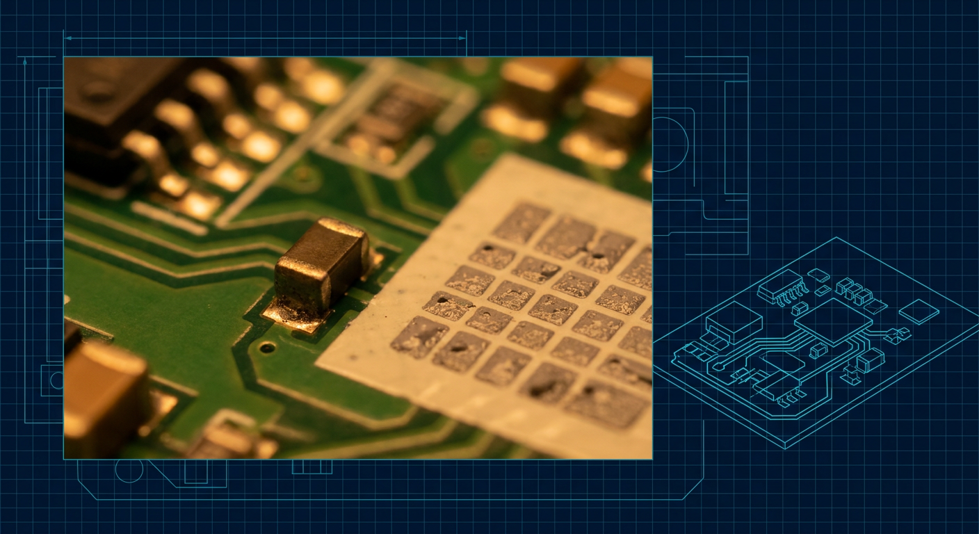
You run DRC in Altium or KiCad, see zero violations, export your ODB++ or Gerber package, and send it to the fab. Four hours later, the fabrication CAM engineer clears the bare-board checks without an engineering question. Three weeks later, your assembled boards arrive from the contract manufacturer, and twenty percent of your 0402 ceramic decoupling capacitors are standing vertically on one pad. Two QFN power management ICs have bridged ground pads underneath the package, and a 2 oz copper MOSFET pad has a cold solder joint that cracked during thermal cycling.
Every single one of those boards passed CAD design rule checks. Every single one passed bare-board CAM screening.
The disconnect comes from a fundamental architectural limitation: EDA design rule checkers evaluate static 2D and 3D geometry against primitive numerical thresholds. Bare-board CAM software like Genesis 2000 or Ucamco UcamX optimizes for etching yield, plating tank currents, and copper layer registration. Neither environment models the fluid dynamics of molten SAC305 solder, the heat transfer differentials across asymmetric copper pours, or the release mechanics of solder paste through a laser-cut stainless steel stencil.
When you are the only hardware engineer on a startup team, an assembly line stoppage or a post-assembly rework cycle eats directly into your runway. Understanding why CAD rules fail to catch assembly defects lets you build defensive layout habits before your files hit the factory.
The Three Distinct Validation Domains
To see why errors slip through, you have to separate the manufacturing pipeline into three distinct validation stages. Each stage uses different software, looks for different physics, and optimizes for different economic outcomes.
First is in-tool EDA Design Rule Checking (DRC). This is a purely geometric verification engine. If you set a rule that trace-to-trace clearance must be at least 0.1 mm (3.94 mil), the DRC engine scans the spatial database and flags any copper vertex that encroaches within that boundary. It does not know whether that 0.1 mm gap is between two high-speed differential pairs or between a solder pad and an unconnected ground flood. It does not know whether a trace will act as a thermal wick during reflow.
Second is bare-board fabrication CAM (Computer-Aided Manufacturing). When your files reach shops like Shengyi, KingCredo, or Advanced Circuits, CAM engineers import your Gerbers into tools like Frontline Genesis 2000, InCAM, or UcamX. The CAM engineer runs automated scripts to modify your data for bare-board fab yield:
- Etch compensation (scaling up trace widths by 0.5 to 1.5 mil to counteract chemical undercut during acid or alkaline etching).
- Acid trap elimination (radiusing or shaving acute copper angles below 90 degrees where etchant can pool and over-etch traces).
- Solder mask optimization (pruning mask slivers below 3 mil that would otherwise peel off in the developer bath and contaminate plating tanks).
- Copper balancing and thieving (adding cross-hatched or solid dummy copper squares to low-density areas to ensure even current distribution during electrolytic copper plating).
Bare-board CAM tools do not check if a component will solder properly on an SMT line. Their job is done if the raw fiberglass and copper panel matches netlist continuity without shorts or opens.
Third is Assembly DFM (Design for Assembly / DFA). This is where the physics of pick-and-place equipment, paste printing, component body tolerances, and convection reflow ovens collide with your board layout. This review is often handled manually by the contract manufacturer (CM) or run through separate, expensive assembly CAM software like Valor NPI or Aegis CircuitCAM. If your CM is a fast-turn prototype house, they often skip deep DFA checks altogether to meet a 24-hour turn, leaving the assembly line to absorb the yield fallout.
+-------------------------------------------------------------------------+
|                         PCB VALIDATION PIPELINE                         |
+-------------------------------------------------------------------------+
| 1. In-Tool EDA DRC      | Static 2D/3D clearances, netlist continuity,  |
|                         | track widths, keepouts.                      |
+-------------------------+-----------------------------------------------+
| 2. Bare-Board CAM       | Etch compensation, acid traps, copper theft,  |
| (Genesis, UcamX)        | mask slivers, panelization plating margins.   |
+-------------------------+-----------------------------------------------+
| 3. Assembly DFM / DFA   | Wetting balance, thermal mass, paste release, |
| (Valor NPI, SMT Line)   | stencil ratios, pick-and-place clearances.    |
+-------------------------+-----------------------------------------------+
SMT Defect 1: 0402 and 0201 Tombstoning
Tombstoning (the Manhattan effect) happens when a two-terminal passive component lifts off one pad during reflow and stands upright. It is caused by an imbalance in the surface tension torque exerted by liquid solder on the two terminations of the part.
During reflow, as the board enters the liquidus phase (roughly 217 degrees Celsius for SAC305), the solder paste melts and wets the metallized terminations of the passive component. The wetting force exerted on each side can be expressed by the Young-Dupre equation relating surface energy and contact angle:
$$F_{\text{wetting}} = \gamma_{\text{LF}} \cdot P \cdot \cos(\theta)$$
Where $\gamma_{\text{LF}}$ is the liquid-flux surface tension, $P$ is the wetted perimeter of the component metallization, and $\theta$ is the contact angle of the molten solder fillet.
If Pad A reaches the liquidus temperature even 0.5 seconds before Pad B, or if Pad A has a larger meniscus of molten solder than Pad B, the wetting force on Pad A will pull down and inward. Pad B, still solid or semi-solid, provides no balancing pull. The component rotates vertically around the edge of Pad A. The result is an open circuit.
                     MOLTEN SOLDER (PAD A)         SOLID / SLOW SOLDER (PAD B)
                   +-----------------------+      +--------------------------+
                   | Wetting force pulls   |      | Incomplete wetting       |
                   | component downward    |      | provides no anchor       |
                   +-----------------------+      +--------------------------+
                                      \                /
                                       \   [0402 CAP] /
                                        \   /======\ /
                                         \ /        /
                                          |        /
                                          |       /
                                   +------+      +------+
                                   |PAD A |      |PAD B |
                                   +------+      +------+
                                   [Heavy Flood] [Thin Trace]
Why DRC Misses It
Your EDA tool sees two pads belonging to the same footprint (for instance, a 0402 ceramic capacitor, metric 1005). Pad 1 connects to +3V3 via a thin 0.2 mm trace. Pad 2 connects directly to an internal GND copper pour through a solid, non-relieved via right at the pad edge, or sits directly embedded inside an outer-layer ground pour.
As far as DRC is concerned:
- Pad-to-pad clearance is 0.5 mm (Pass).
- Trace width meets current capacity rules (Pass).
- Netlist connectivity is verified (Pass).
When the board goes through the convection reflow oven, the massive copper pour connected to Pad 2 acts as a heat sink, siphoning thermal energy away from the pad. Pad 1 has almost zero thermal sink capacity because its thin trace restricts heat conduction. Pad 1 reaches 217 degrees Celsius while Pad 2 is still at 208 degrees Celsius. The paste on Pad 1 melts, wets, and exerts torque. The component tombstones.
How to Fix It at the CAD Level
Do not rely on global thermal relief rules to catch passives. You need explicit design practices for discrete two-terminal parts:
- Enforce trace symmetry. If Pad 1 has a 0.2 mm trace entering it, Pad 2 should have a trace of identical width exiting it for at least 0.5 mm before widening into a power plane or terminating in a via.
- Avoid direct copper flood attachment. If a passive pad must connect to a ground plane on the outer layer, neck down the connection with a short segment of trace (0.2 mm to 0.25 mm wide) or use a thermal relief tie with defined spoke widths.
- Keep vias off the pad unless using filled and capped vias (VIPPO). A standard un-tented or tented via placed 0.1 mm from a passive pad will steal solder through capillary action (wicking), robbing the joint of volume and creating both a thermal and volumetric imbalance.
SMT Defect 2: Thermal Relief Geometry on Heavy Copper
Power electronics boards (motor inverters, DC-DC buck stages, battery protection circuits) often use 2 oz (70 um) or 3 oz (105 um) copper to carry high continuous currents. When laying out high-current paths, engineers frequently disable thermal reliefs, opting for direct, solid connections to copper pours to reduce parasitic resistance and inductance.
For power inductors, high-side MOSFETs (D2PAK, PowerPAK, LFPAK), and large electrolytic bulk capacitors, this causes severe manufacturing failures during both reflow and secondary selective or hand soldering.
+-----------------------+-----------------------+-----------------------------+
| Copper Weight         | Standard Spoke Width  | Recommended Thermal Spoke   |
|                       | (Default EDA)         | for SMT Pads (High Current) |
+-----------------------+-----------------------+-----------------------------+
| 1 oz (35 um)          | 0.20 mm (8 mil)       | 0.25 mm to 0.35 mm          |
| 2 oz (70 um)          | 0.25 mm (10 mil)      | 0.40 mm (use 4x spokes)     |
| 3 oz (105 um)         | 0.30 mm (12 mil)      | 0.50 mm (or necked tie)     |
+-----------------------+-----------------------+-----------------------------+
The Failure Mechanism
When a large multi-pin component has some pins tied directly to a massive internal 2 oz plane and adjacent signal pins connected to isolated traces, two things happen:
First, the solid-connected pins fail to reach solder melting temperature within the standard reflow profile window (typically 60 to 90 seconds above liquidus, peaking at 245 degrees Celsius for SAC305). The paste forms a granular, non-wetted cold joint that might pass initial electrical testing at room temperature but fails under mechanical vibration or thermal expansion in the field.
Second, if through-hole connectors or large power terminals require wave soldering or manual rework, a solid connection makes it impossible to bring the pin to temperature without heating the entire board to 200 degrees Celsius, often blistering the FR4 substrate or destroying adjacent ICs.
Why CAM and DRC Pass It
In Altium, KiCad, or OrCAD, a solid connection is simply a net property. The DRC engine checks that the plane net matches the pin net. It calculates the connection resistance as negligible and reports zero errors.
Bare-board CAM sees a large copper area. To the bare-board fab, large copper areas are easy to etch and plate. They have no reason to flag it.
Practical Thermal Tie Guidelines
If you need low DC resistance but must maintain solderability:
- Use four-spoke thermal ties instead of two-spoke ties, but calibrate spoke width to copper weight.
- For a 2 oz copper board, a four-spoke relief with 0.4 mm (16 mil) spoke widths provides roughly 0.05 mOhm of resistance across the tie while maintaining sufficient thermal impedance to prevent heat siphoning during the 90-second reflow window.
- For bottom-terminated power packages (like QFN power pads), direct connection is necessary for heatsinking, but the paste mask must be modified, not the copper geometry.
SMT Defect 3: Paste Mask Apertures and Voiding on QFNs
One of the most frequent reasons an assembly line halts your prototype run is an unedited solder paste layer on bottom-terminated components (BTCs), quad flat no-lead packages (QFNs), and land grid arrays (LGAs).
By default, most EDA footprint generators export the paste mask layer (Top/Bottom Paste) with a 1:1 ratio to the copper pad. If your QFN has a central 5.0 mm x 5.0 mm exposed ground pad, the CAD tool generates a solid 5.0 mm x 5.0 mm square of solder paste on the stencil.
       DEFAULT EDA PASTE MASK                       CORRECT DFM APERTURE
      (100% Solid Paste Block)                   (Windowpane Array: 60-70%)
      +-----------------------+                  +-----+  +-----+  +-----+
      |                       |                  |     |  |     |  |     |
      |                       |                  +-----+  +-----+  +-----+
      |    SOLID EXPOSURE     |                  +-----+  +-----+  +-----+
      |   Causes Outgassing   |                  |     |  |     |  |     |
      |  Voiding & Component  |                  +-----+  +-----+  +-----+
      |       Floating        |                  +-----+  +-----+  +-----+
      |                       |                  |     |  |     |  |     |
      +-----------------------+                  +-----+  +-----+  +-----+
Stencil Physics: Aspect and Area Ratios
When solder paste is applied via a squeegee across a laser-cut stainless steel stencil, the paste must fill the stencil aperture completely and then release cleanly onto the PCB copper pad when the stencil separates vertically from the board.
This release is governed by the IPC-7525 standard using two mathematical checks:
- Aspect Ratio ($AR$): The width of the aperture ($W$) divided by the stencil thickness ($T$). It must be greater than 1.5.
$$AR = \frac{W}{T} \ge 1.5$$
- Area Ratio ($AreaR$): The surface area of the aperture opening divided by the surface area of the inside aperture walls.
$$AreaR = \frac{L \cdot W}{2 \cdot (L + W) \cdot T} \ge 0.66$$
For a standard 0.127 mm (5 mil) stencil, fine-pitch pads (like 0.4 mm pitch QFN signal leads with a width of 0.2 mm) will fail the area ratio threshold if not compensated, leading to clogged stencil apertures and insufficient solder on peripheral leads.
The QFN Ground Pad Problem
When a solid 100% paste block is printed on a large thermal pad:
- The volatile solvents and flux vehicles inside the solder paste cannot escape during the soak and reflow zones.
- Gas bubbles get trapped under the silicon die, creating thermal voids exceeding 40% to 50% of the pad area. IPC-A-610 Class 2/3 limits thermal pad voiding to 25% or 15% maximum.
- The volume of molten solder lifts the entire component body upward (hydroplaning effect). The peripheral signal leads on the perimeter lift off their pads, creating open circuits or solder bridges between adjacent signal pins.
The Fix: Windowpane Arrays
Never print 100% paste coverage on an exposed center pad. Segment the paste mask into a grid array (windowpane pattern):
- Reduce total paste coverage to between 50% and 70% of the total copper pad area.
- Leave solder mask webbing or unprinted channels (0.15 mm to 0.25 mm wide) between the paste windows. These channels act as outgassing vents for vaporized flux during reflow.
- For a 5.0 mm x 5.0 mm pad, create a 3x3 array of smaller square apertures (e.g., 1.1 mm x 1.1 mm each), separated by 0.2 mm bare gaps.
Modern automated layout platforms are beginning to solve this natively. For instance, IntelCAD (intelcad.ai) handles pad geometry and assembly rules simultaneously, automatically converting solid BTC ground paste exposures into IPC-7525 compliant windowpane arrays during routing rather than forcing the engineer to construct custom paste layers inside footprint libraries.
Solder Mask Webbing: SMD vs NSMD
Solder mask clearances represent another area where bare-board fab rules pass cleanly, but assembly fails with bridging.
There are two ways to define an SMT pad:
- Non-Solder Mask Defined (NSMD): The copper pad is smaller than the solder mask opening. The mask clears the pad on all sides by 0.05 mm to 0.075 mm (2 to 3 mil). This is the standard for almost all surface mount discretes and leaded components because copper etching tolerances (+/- 0.5 mil) are tighter than solder mask registration tolerances (+/- 1.5 to 2 mil).
- Solder Mask Defined (SMD): The solder mask overlaps the copper pad, defining the wettable surface area. This is primarily used for fine-pitch BGAs (0.4 mm pitch and below) to prevent pads from lifting under shear stress and to create a consistent pad shape.
         NSMD (Copper Defined)                      SMD (Mask Defined)
     +---+                      +---+           +=======================+
     |MSK|                      |MSK|           |      SOLDER MASK      |
     +---+                      +---+           +---+               +---+
         |  +----------------+  |                   |  +---------+  |
   Clear |  |   COPPER PAD   |  | Clear             |  | COPPER  |  |
   Area  |  |                |  | Area              |  |   PAD   |  |
  -------+--+----------------+--+-------         ---+--+---------+--+---
                 FR4 SUBSTRATE                        FR4 SUBSTRATE
The Mask Sliver Problem
When routing fine-pitch parts (such as an 0.5 mm pitch QFN or a 0.4 mm pitch WLCSP), the gap between adjacent copper pads is often only 0.2 mm to 0.25 mm (8 to 10 mil).
If you use NSMD pads with a standard 0.05 mm mask expansion:
- The pad gap is 0.20 mm.
- Mask expansion on Pad A subtracts 0.05 mm.
- Mask expansion on Pad B subtracts 0.05 mm.
- The remaining solder mask dam (web) between the two pads is $0.20 - 0.05 - 0.05 = 0.10\text{ mm}$ (3.93 mil).
Most fabrication shops require a minimum solder mask dam of 4.0 mil for green solder mask, and 4.5 to 5.0 mil for matte black, white, or red masks (due to different chemical properties and light diffraction during exposure).
If the mask dam is below the fab threshold, the CAM engineer will simply clip the solder mask dam out entirely (gang mask relief) without asking you, leaving a single wide mask opening across all pins.
When that board hits the SMT line:
- There is no physical solder mask barrier between the adjacent leads.
- Molten solder flows across the bare FR4 between pins.
- Solder bridging occurs across 30% of your fine-pitch pins.
+-----------------------+-----------------------+-----------------------------+
| Mask Color            | Minimum Solder Mask   | Recommended Min Pad Gap     |
|                       | Dam (Factory CAM)     | for NSMD Retention          |
+-----------------------+-----------------------+-----------------------------+
| Standard Green        | 0.075 mm (3.0 mil)    | 0.175 mm (7.0 mil)          |
| Matte Green / Blue    | 0.100 mm (4.0 mil)    | 0.200 mm (8.0 mil)          |
| Matte Black / White   | 0.125 mm (5.0 mil)    | 0.225 mm (9.0 mil)          |
+-----------------------+-----------------------+-----------------------------+
If your pitch is too tight to maintain a reliable mask dam, you must switch the footprint to SMD pads or use a high-resolution LDI (Laser Direct Imaging) solder mask process specified in your fab notes.
A Defensive Layout Checklist Before Exporting Files
Because standard EDA DRC engines do not check assembly-level physics, you need to execute your own assembly review before generating production Gerbers or ODB++ files.
1. Thermal Balance on Discretes
- Isolate every 0201, 0402, and 0603 passive component.
- Ensure traces entering both pads are of identical width for at least 0.5 mm.
- If one pad connects to an outer ground flood, use a necked-down trace rather than a solid pour embedment.
- Check that vias are placed at least 0.25 mm away from passive pad edges unless filled and plated over.
2. Large Copper and Thermal Reliefs
- Check all power nets on 2 oz or 3 oz layers.
- Verify that SMT power pads have thermal relief spokes calibrated to provide thermal impedance during the 90-second reflow window while meeting DC current requirements.
- Verify that through-hole power connector pins have thermal reliefs to allow selective wave soldering without preheating the entire panel.
3. Paste Mask Reduction on BTC/QFN Pads
- Check every central thermal ground pad in your design.
- Ensure the paste mask layer is segmented into a windowpane pattern with 50% to 70% total coverage.
- Ensure the unprinted channels between paste windows are at least 0.15 mm wide to allow flux outgassing.
4. Solder Mask Webbing Verification
- Calculate the actual mask dam width between fine-pitch IC pins ($Gap - 2 \times \text{Expansion}$).
- If the remaining dam is less than 0.1 mm (4 mil), change the solder mask expansion rule to 0.025 mm (1 mil) or switch the pad design to SMD.
- Include an explicit note in your fabrication drawing stating: Solder mask dams must be retained between all IC leads. Gang masking not permitted on pitch <= 0.5 mm without engineering approval.
Running these checks manually takes forty minutes on an eight-layer board. Fixing the same errors after an assembly run takes three weeks of respin time, stencil re-ordering, component re-buying, and assembly line reset fees.