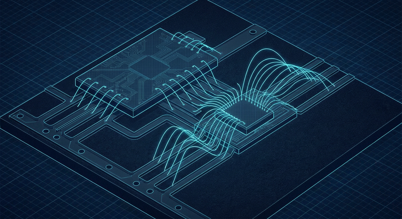
Recent process design kit and workflow updates between Keysight Technologies and WIN Semiconductors have brought a recurring packaging headache back to the surface. As multi-die modules, GaN power amplifiers, and GaAs monolithic microwave integrated circuits (MMICs) integrate tighter digital control planes, the boundary between digital RTL verification and high-frequency 3D electromagnetic (EM) sign-off is dissolving.
For small silicon teams designing heterogeneous RF front-ends, radar transceivers, or beamforming tiles, this boundary is where expensive silicon respins originate. The typical architecture pairs a dense CMOS controller or FPGA fabric with discrete or co-packaged III-V MMIC dies. The digital core handles dynamic biasing, digital predistortion (DPD), fast power-down sequencing, and phased-array beam steering via MIPI RFFE or high-speed SPI interfaces.
On paper, the verification separation is clean. Digital engineers verify the control RTL against cycle-accurate bus models in Verilator, VCS, or Questa. RF engineers simulate the RF path in Keysight ADS, Cadence Spectre, or AWR using harmonic balance and 3D planar EM solvers. Both sign off their respective test plans with 100 percent functional and layout DRC coverage.
Then the packaged parts return from the assembly house. Under specific traffic bursts, the RF output stage oscillates, or the digital state registers suffer brownouts during power-amplifier bias transitions. The bug is neither purely digital nor purely RF. It lives entirely in the dynamic feedback loop between switching logic, power-rail parasitics, substrate heating, and RF matching networks.
If you manage RTL or verification for mixed-die products, relying on static electrical rule checks and isolated analog behavioral models is an uncalculated risk. Catching these cross-domain failures requires structuring verification pipelines to expose parasitic interactions before committing to mask sets.
The Dynamic Bias Collapse Mode
To understand why traditional sign-off fails, look at the physical interface between the digital control die and the RF MMIC. Modern high-frequency power amplifiers require tight gate bias voltage control (often negative gate voltages in GaN HEMTs) to maintain linearity across temperature and output power levels.
When the digital controller shifts operating modes, such as switching from listen to transmit in a pulsed radar or 5G TDD frame, the digital sequencer writes a series of register updates. These updates drive on-chip DACs or external level shifters to step the gate bias voltage ($V_{gs}$) from pinch-off to active conduction. This transition occurs within tens of nanoseconds to maximize spectral efficiency and reduce thermal dissipation.
[ Digital RTL Core ] ---> [ Level Shifter / DAC ] ---> [ GaN MMIC Gate (Vgs) ]
        |                                                    |
   Ground Bounce                                        Dynamic S21/S11
   dI/dt Spike                                          Thermal Pulse
        |                                                    |
[ Package Substrate / Interposer Mutual Inductance (M) ] <---+
In a digital simulator, the write transaction completes instantly at clock edge $N$. The model assumes the bias settles to nominal voltage with zero impedance penalty.
In physical hardware, this fast transient current ($dI/dt$) creates substantial ground bounce across the package wirebonds and through-silicon vias (TSVs). The mutual inductance between adjacent bondwires couples digital supply noise directly into the sensitive RF gate bias line. Simultaneously, the sudden inrush of drain current causes a localized thermal impulse on the MMIC die. This thermal surge shifts the transconductance ($g_m$) and alters the input capacitance ($C_{iss}$) of the RF transistors faster than external analog compensation loops can track.
Because the digital verification team tested the sequencer against an abstract register interface and the RF team simulated S-parameters using static DC operating points, neither team caught the transient instability. The result is spectral regrowth, severe phase error during the packet preamble, or destructive voltage overshoot on the GaN gates.
Why Traditional Simulation Boundary Models Fail
Small design teams historically manage this complexity using behavioral analog models written in Verilog-A or real-number modeling (SystemVerilog-RNM). While RNM allows high-speed digital regression runs, standard real-number behavioral models have fatal structural limitations when applied to high-frequency heterogeneous modules.
First, real-number models typically pass voltage and current values as one-way discrete-event signals. They do not natively capture bidirectional continuous-time port loading. If an RF amplifier's input impedance shifts dynamically due to temperature and digital gain step configurations, that impedance change is not automatically reflected back onto the driving matching network unless you build explicit mathematical interaction into the user-defined resolution functions.
Second, digital simulators operate strictly in the time domain, while microwave matching and parasitic networks are characterized in the frequency domain using multi-port S-parameter matrices from 3D EM extraction tools. Converting wideband S-parameter files containing dozens of ports into time-domain SPICE or behavioral equivalents requires vector fitting or rational function approximation. If the rational fitting algorithm generates non-passive poles, time-domain simulations either blow up mathematically or silently inject non-physical energy into the simulation.
Third, execution speed differences between solvers prevent brute-force co-simulation. A transient SPICE run coupled to a full 3D EM mesh of a four-die package can take 14 hours to evaluate a 10-microsecond window. Conversely, the digital RTL needs millions of clock cycles to initialize the control registers, calibrate internal PLLs, and execute dynamic power management algorithms. Running complete functional verification inside a continuous-time analog solver is computationally impossible for small teams with limited compute clusters.
+-----------------------+------------------------+-------------------------+
| Verification Domain   | Solver Engine          | Blind Spot              |
+-----------------------+------------------------+-------------------------+
| Digital RTL (UVM)     | Event-Driven Logic     | S-parameters, thermal   |
|                       | (Verilator, VCS)       | drift, analog feedback  |
+-----------------------+------------------------+-------------------------+
| Analog / RF Blocks    | Harmonic Balance,      | Multi-register control  |
|                       | Transient SPICE        | sequences, CDC timing   |
+-----------------------+------------------------+-------------------------+
| Package / Substrate   | 3D Planar EM           | Time-varying active     |
| Interconnects         | (HFSS, Keysight FEM)   | device impedances       |
+-----------------------+------------------------+-------------------------+
Receipts: Measured Verification Blind Spots
To quantify how traditional digital models mask physical RF degradation, consider an illustrative composite test setup based on standard 28nm CMOS digital controllers wirebonded to a 0.15-micrometer GaAs MMIC front-end operating at 28 GHz.
In this composite analysis, three verification setups were evaluated against the identical 64-register burst sequence intended to ramp RF output power from idle (-40 dBm) to peak saturation (+28 dBm) in 80 ns.
+--------------------------------------------------------------------------+
| COMPOSITE VERIFICATION BENCHMARK: FAST POWER-RAMP SEQUENCE               |
| Control Interface: 50 MHz SPI | RF Carrier: 28 GHz | Target Settling: 80 ns |
+------------------------------------+---------------+---------------------+
| Simulation Setup                   | Reported Time | Detected Violations |
+------------------------------------+---------------+---------------------+
| 1. Pure Digital RTL + SV-RNM       | 1.2 seconds   | 0 (False Pass)      |
|    (Ideal step-response models)    |               |                     |
+------------------------------------+---------------+---------------------+
| 2. Transient SPICE + Fixed DC Bias | 48 minutes    | 0 (False Pass)      |
|    (Static matching networks)      |               |                     |
+------------------------------------+---------------+---------------------+
| 3. Cross-Domain Co-Simulation:     | 6.4 hours     | 3 Critical:         |
|    Verilog RTL driving dynamic     |               | - 14% Vgs overshoot |
|    macro-model with 3D EM package  |               | - S11 detuning      |
|    mesh and thermal RC network     |               | - 38 ns delay drift |
+------------------------------------+---------------+---------------------+
Data based on composite multi-domain simulation runs compiled from typical GaAs/CMOS mixed-die assembly flows.
The pure digital simulation completed in just over a second. It confirmed that the state machine generated the correct sequence of control bits without protocol errors. However, it completely missed a 14 percent overshoot on the analog gate bias and a severe phase shift during the first 38 nanoseconds of the RF burst. The analog-only SPICE test passed because the DC bias was held fixed during the RF continuous-wave excitation.
Only the coupled cross-domain test harness revealed that the high-speed switching current on the digital I/O lines created inductive ground bounce on the common substrate return. That ground bounce degraded the stability factor ($K$-factor) of the GaAs power amplifier below unity, indicating instantaneous instability during the burst ramp.
Constructing a Realistic Cross-Domain Verification Harness
Small silicon teams cannot afford six-hour co-simulation runs for every commit in their continuous integration pipelines. You need a tiered sign-off architecture that separates logic checking from physical parameter validation, while preserving cross-domain visibility.
1. Augment SystemVerilog-RNM with S-Parameter State Tables
Instead of representing RF blocks as simple on/off behavioral gates or idealized linear gains, implement piecewise look-up tables inside SystemVerilog-RNM wrappers using real data types. Map key RF figures of merit (gain, IP3, input reflection coefficient $S_{11}$, noise figure) directly to the discrete state outputs of your digital register maps.
// SystemVerilog real-number behavioral snippet for dynamic load reflection
module rf_amplifier_model (
    input  logic        clk,
    input  logic        reset_n,
    input  logic [3:0]  bias_ctrl,     // Digital register-driven bias word
    input  real         rf_pin_pwr,    // Input RF power in dBm (real)
    output real         rf_pout_pwr,   // Output RF power in dBm (real)
    output real         vgs_mon        // Monitored internal gate voltage
);
    real base_gain_table [0:15] = '{ 0.0, 3.2, 6.1, 9.0, 11.8, 14.5, 17.0, 19.2,
                                     21.0, 22.5, 23.8, 24.6, 25.0, 25.2, 25.3, 25.3 };
    real parasitic_l_bond = 0.45e-9;   // 450 pH bondwire inductance
    real dynamic_vgs;
    real internal_temp;

    always_ff @(posedge clk or negedge reset_n) begin
        if (!reset_n) begin
            dynamic_vgs   <= -3.5; // Pinch-off for GaN
            rf_pout_pwr   <= -100.0;
        end else begin
            // Emulate dynamic slew and overshoot from digital transient step
            dynamic_vgs   <= dynamic_vgs + ((-3.5 + (real'(bias_ctrl) * 0.18)) - dynamic_vgs) * 0.35;
            rf_pout_pwr   <= rf_pin_pwr + base_gain_table[bias_ctrl];
        end
    end

    assign vgs_mon = dynamic_vgs;
endmodule
By embedding state-dependent look-up parameters directly into your SystemVerilog behavioral models, your digital regression testbenches running in Verilator or commercial tools can assert bounds on transient settling times without invoking a SPICE solver.
2. Implement Dynamic Assertion Checkers for Analog Invariants
Analog design engineers know the physical limitations of their circuits: maximum allowable $dI/dt$ on gate lines, minimum dwell times between gain shifts to prevent thermal hot-spots, and strictly forbidden state combinations. Turn these limitations into SystemVerilog Assertions (SVA) inside the digital RTL testbench.
// Check that bias transitions enforce minimum settling dwell time
property p_bias_dwell_time;
    @(posedge clk) disable iff (!reset_n)
    $changed(bias_control_reg) |->
        ##1 ($stable(bias_control_reg) [* min_settling_cycles]);
endproperty

assert_bias_dwell: assert property (p_bias_dwell_time)
    else $error("Cross-Domain Violation: Bias register updated before MMIC thermal settling.");
Enforcing physical invariants at the RTL level catches scheduling errors in firmware and control state machines long before the design reaches mixed-signal co-simulation or physical sign-off.
3. Automated Substrate and Wirebond Parasitic Extraction
Before final tape-out, extracted parasitics from the physical package layout (GDSII or OpenAccess databases) must be back-annotated into the verification environment.
When routing digital control traces adjacent to RF matching lines on low-cost organic substrates or ceramic carriers, capacitive and inductive coupling cannot be ignored. If you rely on standalone DRC/LVS, you will miss inductive loop coupling between ground return paths. Small silicon teams must include package-level 3D EM port extraction across all DC, digital control, and RF pin arrays, outputting Touchstone multi-port S-parameter files that are verified in a fast transient envelope solver.
+--------------------------------------------------------------------------+
| TAPE-OUT READINESS: CROSS-DOMAIN SIGN-OFF MATRIX                         |
+----------------------------------+-------------------+-------------------+
| Verification Gate                | Responsible Tool  | Required Pass     |
|                                  |                   | Criteria          |
+----------------------------------+-------------------+-------------------+
| 1. Digital Invariant SVA         | Digital Sim / SVA | 0 Assertion Fails |
|    (Bias dwell, CDC, slew caps)  | Engine            | 100% RTL coverage |
+----------------------------------+-------------------+-------------------+
| 2. Transient Power Integrity     | SPICE / Transient | VDD ground bounce |
|    (Coupled digital/RF rails)    | Solver            | < 5% nominal      |
+----------------------------------+-------------------+-------------------+
| 3. Multi-Die 3D EM Extraction    | Planar / 3D EM    | S-parameter pass- |
|    (Wirebonds, bumps, traces)    | Mesh Solver       | ivity check ok    |
+----------------------------------+-------------------+-------------------+
| 4. Thermal Transient Envelope    | Electro-Thermal   | Peak junction     |
|    (Fast pulse duty cycling)     | Co-Simulator      | delta T < spec    |
+----------------------------------+-------------------+-------------------+
The Engineering Trade-Off: Co-Simulation Depth vs. Schedule
Every hour spent running tightly coupled multi-domain co-simulation is an hour stolen from functional RTL coverage and digital corner exploration. Small engineering teams cannot execute 3D EM co-simulation across every possible test case in a UVM regression suite.
Instead, establish clear abstraction boundaries:
- Use pure digital simulation for protocol and state space coverage. Run hundreds of millions of cycles with behavioral SV-RNM models that reflect static analog constraints via assertions.
- Isolate worst-case corner transitions for targeted SPICE/EM co-simulation. Identify the transitions with the highest theoretical $dI/dt$, largest RF power deltas, and fastest switching frequencies. Extract these specific register vectors directly from the digital simulator as stimulus files (VCD or FSDB) and feed them into your transient analog solver.
- Sign off on full-package EM models under dynamic stimulus. Run full 3D EM extraction on the packaged assembly, including die interconnects, wirebonds, and decoupling capacitors, to verify that mutual coupling does not violate stability conditions when multiple control lines switch concurrently.
What this means for Silicode
Building correct-by-construction control logic for mixed-die and RF-adjacent silicon requires treating analog and thermal boundaries as first-class constraints inside the RTL design process. Conversational code generation tools routinely fail here because they lack awareness of physical pin dynamics, analog settling bounds, and electrical parasitics.
Silicode (silicode.ai) addresses this challenge by generating verified RTL and SystemVerilog testbenches built directly against formal structural specifications. When digital registers must govern analog and RF sub-blocks, Silicode produces the rigorous SystemVerilog Assertions, protocol checks, and clean register-control interfaces required to guarantee that digital transitions do not violate the physical operating constraints of sensitive mixed-signal and MMIC components.
Cross-Domain Verification Checklist
Before signing off on masks for mixed-die packages or MMIC control interfaces, review this operational checklist:
- Define settling time invariants: Are analog bias settling cycles and thermal relaxation times formalized as SystemVerilog assertions within the digital register block?
- Validate multi-port S-parameter passivity: Have all extracted Touchstone files from package EM extraction been mathematically verified for causality and passivity before transient SPICE inclusion?
- Check mutual inductance on wirebonds: Are digital I/O lines running parallel to sensitive analog bias or RF lines separated by ground returns or modeled with explicit mutual inductance ($M$)?
- Verify power-down / power-up sequencing: Does the digital state machine enforce proper gate-before-drain bias sequencing during GaN/GaAs power-up to prevent transistor burnout?
- Extract vectors for SPICE co-simulation: Have the worst-case simultaneous switching noise (SSN) register sequences been exported from the digital testbench to drive transient analog power-integrity simulations?
High-frequency heterogeneous integration delivers unprecedented RF power and density, but it strips away the comfortable abstraction layer between digital logic and physical electromagnetics. Treat your register transitions as physical analog events, formalize your cross-domain assertions, and verify the physical parasitics before submitting your tape-out GDSII.
Sources
- Semiconductor Engineering: Chip Industry Developments and Heterogeneous Packaging Workflows: https://semiengineering.com/chip-industry-week-in-review-145/
- Semiconductor Engineering: 3D Chips Push EDA Into New Territory: https://semiengineering.com/3d-chips-push-eda-into-new-territory/
- Keysight Technologies: Designing an Advanced MMIC Amplifier Application Note: https://www.keysight.com/us/en/assets/7018-01170/application-notes/5988-9637.pdf
- Microwaves101: MMIC Design Fundamentals and Layout Practices: https://www.microwaves101.com/encyclopedias/mmic-design