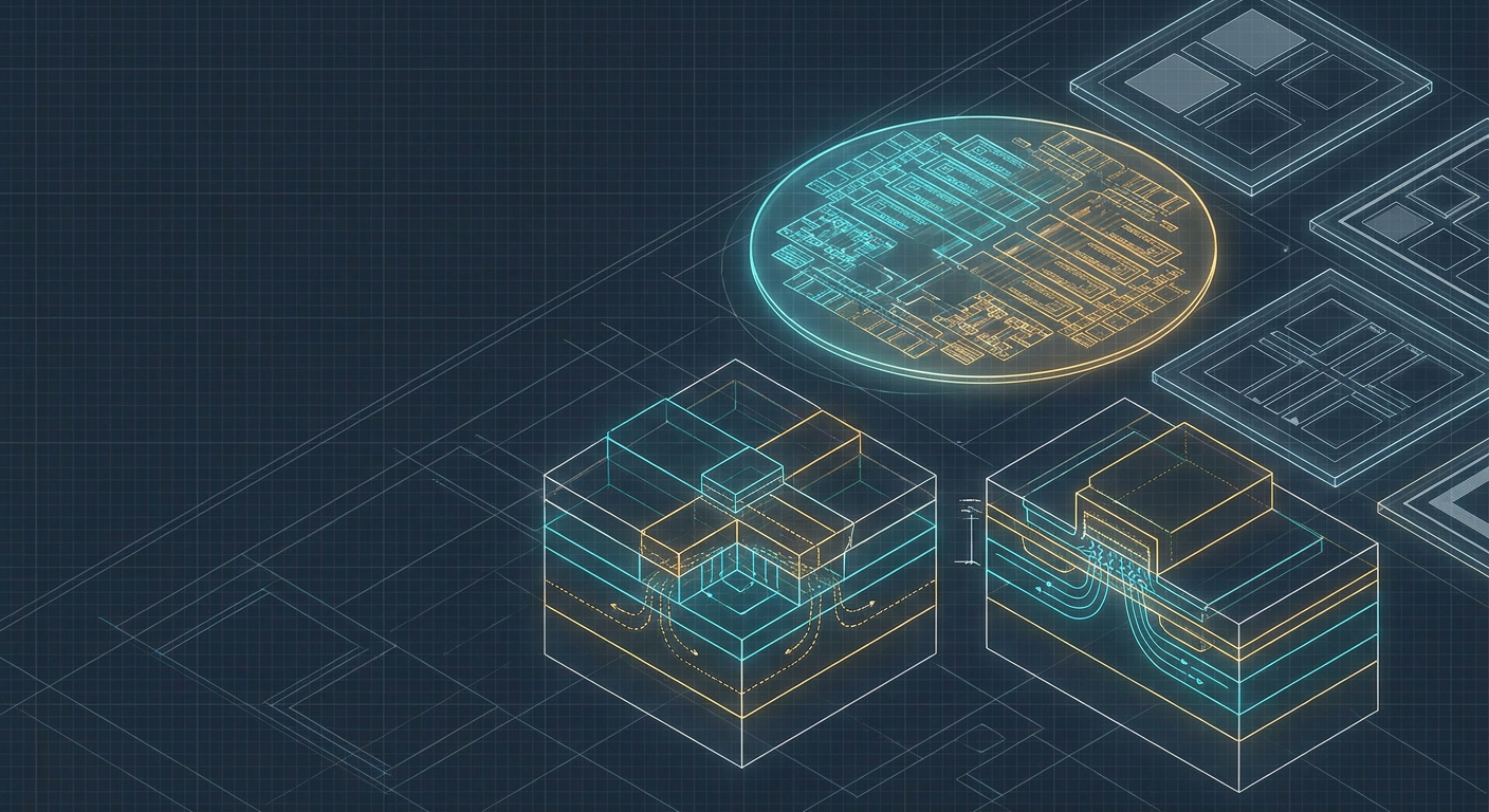
GlobalFoundries announced it will operate two new 300mm wafer fabrication facilities at its Malta, New York campus under a joint United States and Japan initiative backed by up to 21 billion dollars in planned funding. An initial 10 billion dollar phase is moving forward as federal CHIPS Act allocations conclude. While headlines focus on geopolitical reshoring, the immediate engineering consequence for fabless startups, edge AI accelerator teams, and small silicon design offices is practical. It adds long-term domestic capacity for differentiated, mature nodes, specifically 22FDX and 12nm FinFET.
For engineering leads managing budgets, headcount, and tape-out schedules, this expansion clarifies a critical node selection choice. Teams designing low-power edge accelerators, mixed-signal sensor hubs, and motor controllers often face an artificial dilemma: stay trapped in expensive high-end FPGAs, or spend tens of millions of dollars targeting leading-edge TSMC N5 or N4 processes. The Malta capacity build-out reinforces why mature planar FD-SOI and intermediate FinFET nodes remain the actual economic sweet spot for edge hardware.
Taking advantage of 22FDX or 12nm requires understanding the real cost structures, physical trade-offs, and verification bottlenecks. A low mask cost means nothing if your multi-voltage power domains fail sign-off or your RTL produces silent race conditions across power-state transitions.
The Node Economics of Edge Accelerators
Most edge inference workloads do not need three-nanometer logic density. An edge vision pipeline running an 8-bit quantized convolutional network or a lightweight transformer model at 15 to 30 frames per second is constrained by thermal dissipation, memory bandwidth, input-output integration, and bill-of-materials cost.
When a team prototypes an accelerator on an AMD Xilinx Zynq UltraScale+ or a Kria SOM, the unit economics work for low-volume industrial runs. Once product volume targets exceed 25,000 to 50,000 units per year, FPGA component costs devastate unit margins. A mid-tier FPGA device costs anywhere from 120 to 450 dollars in modest volumes. Moving to an ASIC becomes an economic necessity.
Targeting a sub-7nm node for an edge device introduces crippling non-recurring engineering costs. A full mask set at 5nm exceeds 15 million dollars. Adding electronic design automation tooling licenses, third-party IP blocks such as PCIe Gen5 PHYs or LPDDR5 controllers, and dedicated physical design engineering contracts pushes initial tape-out costs beyond 30 million dollars. To break even on that investment against an FPGA baseline, a team must ship millions of units. For industrial automation, aerospace, automotive microcontrollers, and specialized edge robotics, those volume numbers do not exist.
Mature nodes shift the equation completely. A 22FDX mask set costs between 450,000 and 750,000 dollars depending on metal layer stack configurations. A 12nm FinFET mask set sits between 1.2 million and 2.2 million dollars. Multi-project wafer runs drop initial prototype silicon costs even further, often down to 35,000 to 90,000 dollars for a dedicated engineering slot. At these rates, an ASIC transition breaks even at tens of thousands of units rather than millions.
+-----------------------------------------------------------------------------------------+
| ASIC Breakeven Threshold vs High-End FPGA ($180 BOM)                                   |
|                                                                                         |
|  ASIC Total Investment (Mask + Tooling + NRE)                                           |
|  ===========================================                                            |
|  (FPGA Unit Cost - ASIC Unit Die/Pkg Cost)                                              |
|                                                                                         |
|  - 5nm FinFET ($32M NRE / $165 margin delta)  --> ~194,000 units minimum breakeven      |
|  - 12nm FinFET ($4.2M NRE / $162 margin delta) --> ~26,000 units minimum breakeven       |
|  - 22FDX FD-SOI ($1.8M NRE / $164 margin delta) --> ~11,000 units minimum breakeven     |
+-----------------------------------------------------------------------------------------+
22FDX Physics: Body Biasing Versus FinFET Density
The choice between 22nm Fully-Depleted Silicon-on-Insulator and 12nm bulk FinFET is not just about price. It is an architectural decision dictated by transistor physics, power management, and analog integration.
In standard bulk CMOS and 3D FinFETs, the transistor channel connects directly to the silicon substrate. Controlling leakage current requires complex doping profiles or wrapping the gate around a raised silicon fin. In 22FDX, an ultra-thin layer of silicon sits on top of a thin buried oxide dielectric layer. The channel is fully depleted without dopants, eliminating dopant fluctuation noise and dramatically reducing parasitic capacitance.
Forward and Reverse Body Biasing
The primary technical asset of 22FDX is software-controlled body biasing. Because the buried oxide isolates the transistor channel from the base substrate, engineers can apply an independent voltage bias to the back gate beneath the oxide.
- Forward Body Bias: Applying a positive voltage to the back gate of NMOS transistors and negative voltage to PMOS lowers the threshold voltage. This boosts drive current by up to 25 percent, letting an edge DSP or systolic array hit high clock frequencies during burst inference without raising the main supply voltage.
- Reverse Body Bias: Applying a negative voltage to the back gate of NMOS and positive voltage to PMOS raises the threshold voltage. This cuts standby subthreshold leakage current by up to an order of magnitude when the accelerator sits idle between sensor frames.
In a battery-powered sensor hub or an automotive camera processor that wakes up every 100 milliseconds to run an inference pass, body biasing lets you match 16nm FinFET dynamic performance while maintaining sub-milliwatt sleep states.
Mixed-Signal and Radio Frequency Integration
Edge processors rarely live in digital isolation. They interface with MIPI D-PHY camera sensors, radar front-ends, Wi-Fi radios, and precision analog-to-digital converters.
FinFET processes present notoriously difficult analog design challenges. FinFETs offer massive transconductance for digital switching, but their high output conductance, poor intrinsic gain, and quantized fin widths make high-linearity analog circuits painful to layout and verify.
In contrast, 22FDX behaves like high-performance planar silicon with high transconductance-to-current ratios, high maximum oscillation frequencies above 300 GHz, and low flicker noise. Designers can combine a RISC-V control core, an INT8 tensor array, power management units, and an integrated sub-gigahertz or 2.4 GHz RF transceiver on a single monolithic die without discrete off-chip analog stages.
The Verification Trap of Multi-Voltage Power Domains
While 22FDX offers immense power efficiency, it introduces severe verification challenges. To extract the power benefits of FD-SOI, your digital design cannot run on a single clock and static voltage rail. You must implement multiple power domains, dynamic voltage and frequency scaling, retention memory arrays, and adaptive body bias controllers.
This is where many small fabless teams fail. They write standard Verilog or SystemVerilog, verify logical correctness in a basic simulator, and assume the synthesis and place-and-route tools will handle the low-power infrastructure.
In reality, low-power sign-off is governed by Unified Power Format specifications (IEEE 1801). Every power domain switch, isolation cell, level shifter, and state-retention flip-flop must be verified across dynamic operational transitions.
+-----------------------------------------------------------------------------------------+
| Low-Power Physical Implementation Architecture                                          |
|                                                                                         |
|  +-----------------------------+           +-----------------------------------------+  |
|  | Core Always-On Domain       |           | Switchable Accelerator Domain (22FDX)   |
|  | VDD_CORE = 0.8V             |           | VDD_SW = 0.4V to 0.8V                   |
|  | Back-Bias = Static GND      |           | Back-Bias = Dynamic FBB/RBB Controller  |
|  |                             |           |                                         |
|  |   [State Machine]           |  Signals  |   [Matrix Multiply Unit]                |
|  |          |                  | --------> |              |                          |
|  |          |                  |  (Level   |              v                          |
|  |          v                  |  Shifter) |   [Retention Flip-Flops]                |
|  |   [Power Controller]        |           |              |                          |
|  |          |                  | <-------- |              v                          |
|  |          +--(ISO Enable)----+  (ISO)    |   [Power Gate Header Switch]            |
|  +-----------------------------+           +-----------------------------------------+  |
+-----------------------------------------------------------------------------------------+
The Failure Modes of Power Intent Verification
When an edge tensor accelerator shifts from active forward body bias down to a sleep state, several failure modes occur if power intent is not verified alongside functional RTL:
- Isolation Clamping Glitches: When the switchable power domain shuts down, its output signals float into an undefined state. If the isolation enable signal from the power management controller does not assert prior to rail collapse, floating intermediate voltages penetrate the always-on domain. This causes crowbar currents and latch-up conditions.
- Level Shifter Domain Crossings: Stepping down voltage from an always-on 0.8V control bus to a 0.4V near-threshold processing element requires dedicated level shifters. Static timing analysis engines must compute delay variations across both asymmetric rails. An unverified transition time can turn what looks like clean synchronous timing into a hold-time violation on silicon.
- Retention Restoration Clocks: Saving register state prior to power gating requires rigorous sequencing. If clock gates drop after the save trigger or if the restore signal deasserts out of phase with the primary clock tree reactivation, state-retention registers capture corrupted internal buses.
Basic simulation engines running vanilla Verilog do not model power switches, isolation behavior, or floating node penalties. If your verification flow relies on simple testbenches that test only functional arithmetic, these bugs escape directly into physical GDSII layout.
Cost and Schedule Comparison: 22FDX vs 12nm vs Leading-Edge
To frame the trade-offs facing an engineering manager or technical founder, consider a representative low-power edge computer vision inference ASIC. The design targets 4 TOPS of INT8 compute, 2MB of on-chip SRAM, an embedded 64-bit RISC-V application core, and a MIPI CSI-2 camera receiver.
The figures below represent an illustrative composite of typical multi-project wafer and full-mask tape-out parameters across current foundry offerings.
| Parameter | GlobalFoundries 22FDX | GlobalFoundries 12LP+ | TSMC N5 / N4 (Leading Edge) |
|---|---|---|---|
| Transistor Architecture | Planar FD-SOI | 3D FinFET | 3D FinFET / Nanosheet |
| Logic Density (MTr/mm²) | ~35 - 42 | ~85 - 105 | ~220 - 280 |
| Nominal Core Voltage | 0.8V (down to 0.4V) | 0.8V | 0.65V - 0.75V |
| Typical Mask Set Cost | $500k - $750k | $1.4M - $2.2M | $14M - $22M |
| Dedicated MPW Slot (25mm²) | $45k - $75k | $120k - $190k | $600k - $1.2M |
| Typical EDA Tooling Tier | Mid/Standard | High-end Signoff | Advanced Node Complete |
| Body Biasing Capability | Yes (Dynamic FBB/RBB) | No | No |
| Mixed-Signal / RF Feasibility | High (Native on-chip) | Moderate | Complex / Expensive |
| Minimum Production Run Breakeven | 10k - 25k units | 25k - 75k units | >500k units |
Note: Illustrative composite derived from standard fabless foundry broker rate cards, physical design service estimates, and publicly available MPW aggregator pricing.
Looking at the composite data, 12nm FinFET is the correct choice when your design is pure digital logic with a massive memory footprint that requires high gate density to minimize total die area. However, if your design requires mixed-signal front-ends, ultra-low standby power, or tight battery-operated thermal budgets, 22FDX provides equivalent functional power efficiency at less than half the mask set investment.
Why Plausible RTL Breaks on Physical Implementation
The recent trend toward automated code generation in digital design has exacerbated the gap between simulated Verilog and tape-out-ready silicon. Large language models and prompt-based assistants generate synthesizable structural Verilog for standard arithmetic units, finite state machines, and basic interconnect bridges. They excel at writing code that compiles without syntax errors and passes basic functional tests in Verilator or Icarus Verilog.
However, mature FD-SOI and FinFET implementation requires code structured for strict physical constraints:
Metastability and Multi-Clock Domains
Edge accelerators typically ingest data from a camera sensor running on an independent pixel clock, process it across an array of tensor cores running on a variable-frequency system clock, and deliver results to an external host over SPI or PCIe.
Automated code generators frequently instantiate simple two-flop synchronizers without checking for multi-bit bus coherency. Passing a multi-bit pointer across asynchronous clock boundaries using individual flip-flops causes data corruption when bits arrive across different clock edges. A reliable design requires gray-code pointers or asynchronous FIFOs with formal proofs verifying that read and write pointers never cross improperly under any clock phase relationship.
// INSUFFICIENT: Naive multi-bit synchronizer produced by LLM assistants
always_ff @(posedge clk_dest) begin
    sync_stage1 <= async_data_bus; // Bit skew causes transient illegal states
    sync_stage2 <= sync_stage1;
end

// REQUIRED: Handshake or Gray-coded FIFO pointer synchronization
module cdc_gray_sync #(
    parameter int WIDTH = 4
)(
    input  logic             clk_dest,
    input  logic             rst_n,
    input  logic [WIDTH-1:0] async_gray_in,
    output logic [WIDTH-1:0] sync_gray_out
);
    (* ASYNC_REG = "TRUE" *) logic [WIDTH-1:0] stage1_reg, stage2_reg;
    always_ff @(posedge clk_dest or negedge rst_n) begin
        if (!rst_n) begin
            stage1_reg    <= '0;
            stage2_reg    <= '0;
            sync_gray_out <= '0;
        end else begin
            stage1_reg    <= async_gray_in;
            stage2_reg    <= stage1_reg;
            sync_gray_out <= stage2_reg;
        end
    end
endmodule
Clock Gating and Power Architecture
To meet power targets on 22FDX, dynamic clock gating must be inferred at the register level. If the RTL uses monolithic case statements with missing default branches or registers that continually assign their own output, the logic synthesis tool cannot map them to Integrated Clock Gating (ICG) cells from the foundry standard cell library.
Unstructured RTL forces synthesis engines to insert multiplexer feedback loops instead of true clock gates. This keeps the clock tree toggling every cycle, burning dynamic power and defeating the purpose of choosing an FD-SOI process.
A Decision Framework for Edge Silicon Teams
If you are planning an edge silicon roadmap over the next 12 to 24 months, use this structured checklist before committing to an architecture or signing foundry non-disclosure agreements:
- Quantify the Analog-to-Digital Ratio: If your die is over 30 percent analog, radio frequency, or specialized I/O, lean toward 22FDX. The mask savings and simplified mixed-signal layout will offset minor digital area penalties.
- Audit Total Volume Projections: If your realistic year-two shipping volume sits below 100,000 units, avoid sub-10nm FinFET. Use 22FDX or 12nm to prevent your non-recurring mask amortization from destroying gross margins.
- Validate UPF and Power Intent Early: Do not defer power intent verification to the physical design handoff. Simulate your power state table, isolation logic, and retention registers in your functional verification suite before touching synthesis.
- Mandate Formal Lint and CDC Sign-Off: Run automated linting tools and formal clock domain crossing verification on every module. Catch inferred latches, width mismatches, and unsynchronized crossings before generating netlists.
- Plan MPW Validation Prototypes: Budget for an intermediate multi-project wafer run to validate PLL locks, high-speed PHY interfaces, and analog biasing loops before committing to a full production mask set.
What This Means for Silicode
Silicode builds verification-first automation tools for RTL generation and ASIC workflows. As foundry capacity expands across mature nodes like 22FDX and 12nm, the bottleneck in silicon development shifts from wafer availability to front-end engineering throughput and verification closure.
Silicode is built on the reality that generating syntactically valid Verilog is not enough. Production silicon requires verified RTL supported by automated testbench generation, strict linting, formal assertions, and full power-intent validation. By tying generative RTL pipelines directly to deterministic simulation engines and formal verification harnesses, Silicode helps small silicon teams deliver tape-out-grade designs that pass physical sign-off without costly re-spins.
Practical Steps for Engineering Leads
Keep a close eye on foundry capacity roadmaps as GlobalFoundries breaks ground on the new Malta facilities. If you are currently shipping an FPGA-based appliance or industrial controller, begin running synthesis and area estimation benchmarks on mature FD-SOI and FinFET standard cell libraries now.
Do not wait for your production volumes to suddenly demand an ASIC. Set up clean RTL repositories with explicit clock domain definitions, clean synchronous resets, and modular power-domain boundaries. When your volume reaches the economic transition threshold, having verification-hardened code ready for physical synthesis is the difference between hitting your market window and burning your runway on avoidable engineering re-spins.
Direct Q&A
What makes 22FDX and 12nm more practical for edge silicon than leading-edge nodes?
Leading-edge nodes (sub-7nm) carry mask set and tooling costs exceeding 20 million dollars, requiring multi-million-unit production runs to break even. Mature nodes like 22FDX and 12nm offer mask sets under 2 million dollars, lower MPW entry costs, superior analog/RF integration, and dynamic body biasing for ultra-low standby power, making them economically viable for edge volumes between 10,000 and 100,000 units.
How does body biasing on 22FDX reduce power consumption?
22FDX isolates the transistor channel with a thin buried oxide layer, allowing designers to apply an independent voltage bias to the back gate. Forward Body Bias lowers threshold voltage to boost performance during active compute bursts without raising supply voltage. Reverse Body Bias raises threshold voltage to reduce standby leakage current by up to 10x during idle periods.
Sources
- GlobalFoundries Malta Expansion: https://gf.com/news-and-events/news/globalfoundries-selected-to-operate-two-new-semiconductor-fabs-in-new-york-under-landmark-us-japan-initiative/
- Congressional Research Service CHIPS Act Facility Funding: https://www.congress.gov/crs_external_products/R/PDF/R49031/R49031.1.pdf
- GlobalFoundries FDX Technology Platform: https://gf.com/technologies/cmos/fdx-fd-soi/
- CMC Microsystems 22FDX Technology Description: https://www.cmc.ca/globalfoundries-22fdx-fdsoi-22-nm/
- IEEE 22FDX IoT and Automotive Overview: https://ieeexplore.ieee.org/document/9320648/
- GlobalFoundries and NXP 22FDX Deployment: https://gf.com/news-and-events/news/globalfoundries-and-nxp-to-deliver-next-generation-22fdx-solutions-for-automotive-iot-and-smart-mobile/
- Foundry Node Comparison (AnySilicon): https://anysilicon.com/tsmc-22nm-vs-umc-22nm-vs-gf-22fdx/