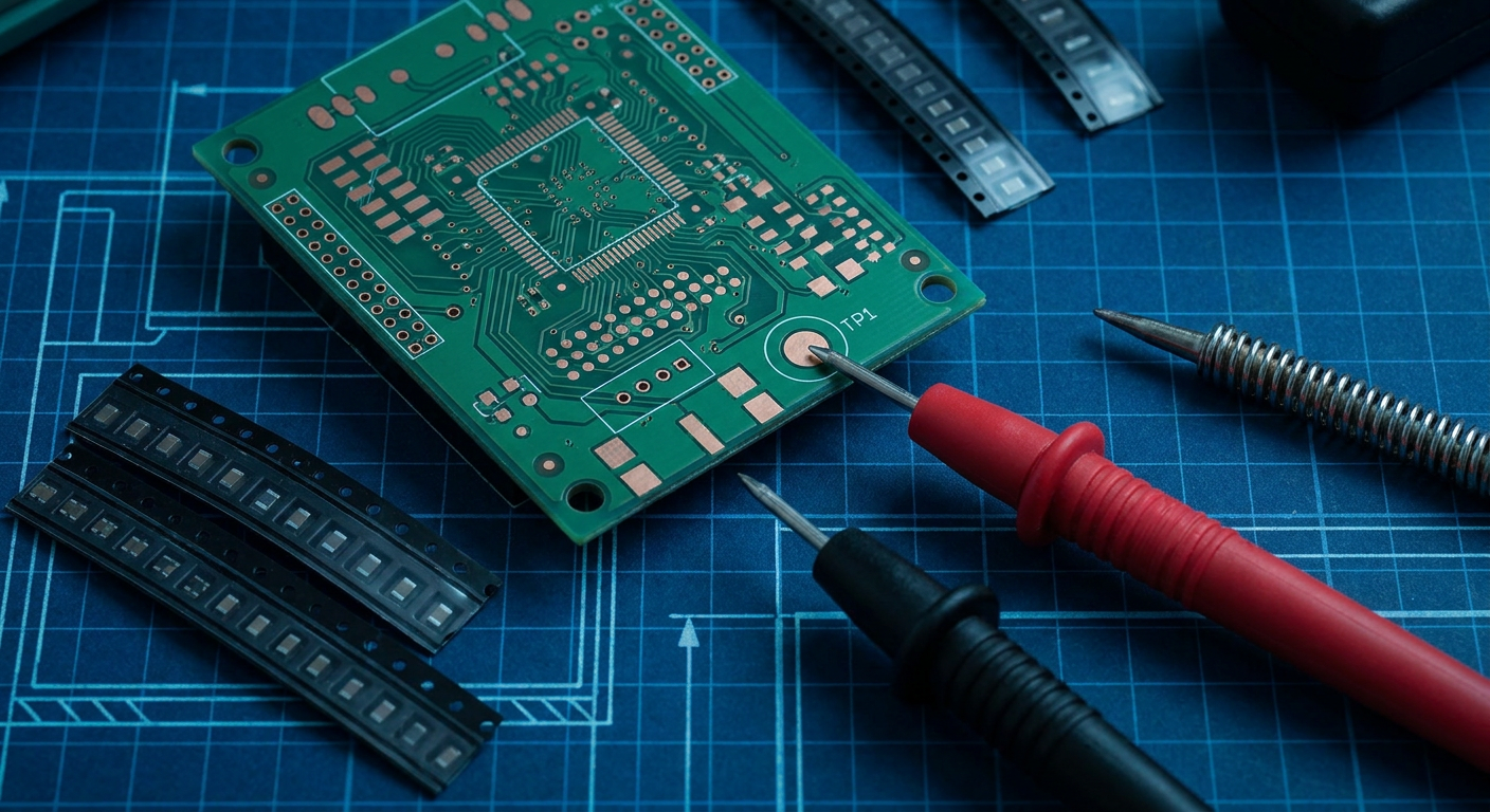
Industry survey data from hardware prototyping studies highlights a persistent baseline in electronic product development: the average commercial PCB project requires 2.9 board spins before reaching stable production. For a solo hardware engineer or a small engineering team inside an early-stage hardware company, a revision cycle is rarely just a line item for $350 in bare boards and $800 in quick-turn SMT assembly. The real expense hides in downstream stall time, bench rework under a microscope, blocked firmware development, and slipped customer validation milestones.
When a revision arrives with a dead power rail or an inverted pinout on an IC, the board invoice is negligible compared to the operational burn rate. If three engineers are blocked for 14 days waiting on a corrected fabrication batch, that delay easily consumes $20,000 to $50,000 in operational payroll while critical project deadlines slip. Understanding where prototype tapeouts break, how rework compares to a full refabrication, and which checks eliminate the most destructive errors is the only way to keep hardware schedules on track.
Where Early Tapeouts Actually Fail
Most prototype respins do not fail because of complex electromagnetic field interactions or exotic multi-gigabit signal degradation. Those problems happen on high-density computing platforms, but the majority of day-one bringup failures on 2-layer to 6-layer microcontroller and sensor boards stem from pedestrian errors in schematic capture, component footprints, and system-level connectivity.
+-------------------------------------------------------------------------+
| TYPICAL BRINGUP FAILURE DISTRIBUTION (ILLUSTRATIVE COMPOSITE)           |
+------------------------------------+------------------------------------+
| Failure Category                   | Primary Mechanism                  |
+------------------------------------+------------------------------------+
| Footprint & Pin Mapping Inversions | Swapped TX/RX, mirrored QFN pads,  |
|                                    | reversed diode polarities          |
| Power Distribution & Sequencing    | Enable pull-ups on unpowered rails,|
|                                    | missing bulk caps, dropouts        |
| Connector Mechanical & Polarities  | Mirrored ribbon headers, wrong     |
|                                    | mating orientation, zero clearance |
| SMT Assembly Clearances            | Solder bridging on 0.4mm pitch ICs,|
|                                    | tombstoning on unshared thermals   |
+------------------------------------+------------------------------------+
The composite breakdown above reflects the common culprits documented across hardware post-mortems and assembly house audits. Three specific failure modes account for a disproportionate share of scrapped prototype batches.
1. Reversed Diode and Transistor Footprints
Component packaging conventions remain inconsistent across discrete component manufacturers. An SOD-123 or SMA diode footprint from one vendor library may define Pin 1 as the cathode, while another CAD library defines Pin 1 as the anode. Silk screen line markings on small surface-mount diodes are notoriously ambiguous under optical inspection.
When a protection diode or Schottky barrier diode is placed backward on a power input rail, the power rail shorts directly to ground through the forward-biased junction the moment the bench supply is switched on. If the bench power supply does not have its current limit dialed down below 100 mA, the trace fuses, the diode package cracks, or the upstream regulator is destroyed before firmware can even begin execution.
2. Misplaced Power Sequencing Nets and Floating Resets
Modern microcontrollers, wireless system-on-chips, and power management ICs (PMICs) demand specific power-on reset timings and multi-rail sequencing. A common schematic error occurs when an active-low reset pin or enable net is tied through a pull-up resistor to a secondary regulated rail that powers up hundreds of milliseconds after the main input voltage.
The microcontroller enters a brownout or latch-up state because its reset line sits at an undefined intermediate voltage while the core logic tries to boot. Debugging this on the bench often consumes three days of oscilloscope probing, only to discover that the fix requires cutting an internal trace and running a blue jumper wire from the reset pull-up to the primary 3.3V rail.
3. Mirrored and Rotated Connector Pinouts
Connectors are the single largest source of mechanical respins. The schematic symbol for a dual-row 10-pin header often presents a clean top-down logical view, but connector vendors vary on whether pin numbers proceed zig-zag (1-2-3-4 across rows) or consecutively down one side (1-3-5 on the left, 2-4-6 on the right).
A board designed against a top-entry header footprint that gets substituted with a right-angle counterpart will invert odd and even rows relative to the cable harness. Connecting a ribbon cable to a mirrored SWD or JTAG debug header immediately sends 3.3V into a ground pin and ground into a high-speed clock line, permanently disabling the debug port on the target microcontroller.
The Direct Mathematics of a Slipped Revision
A solo engineer building hardware often assumes a two-week turn delay is simply two weeks added to the end of the roadmap. In practice, hardware development runs on interlocked dependencies across electrical, mechanical, and software domains.
+-------------------------------------------------------------------------+
| TWO-WEEK RESPIN IMPACT AUDIT (ILLUSTRATIVE COMPOSITE RUN)               |
+------------------------------------+------------------------------------+
| Cost Category                      | Estimated Financial Impact         |
+------------------------------------+------------------------------------+
| Expedited PCB Fab + Assembly (5pcs)| $1,200 to $2,500                   |
| Scrapped SMT Components & Bare Bds | $300 to $900                       |
| Bench Debug & Blue-Wire Rework     | 24 hours @ $125/hr = $3,000        |
| Blocked Firmware Engineers (2 devs)| 80 hours @ $95/hr = $7,600         |
| Delayed Mechanical Enclosure Fit   | Tooling freeze slip = $4,500       |
| Slipped Field Pilot Demonstration  | Commercial milestone risk          |
| Total Quantifiable Run Impact      | $16,600 to $18,500+                |
+------------------------------------+------------------------------------+
The financial figures in the table above represent standard mid-market startup overhead, combining raw fab charges with typical engineering labor rates. When bare boards arrive non-functional, the hardware engineer spends 20 to 30 hours under a stereo microscope with a scalpel, Kapton tape, and 30 AWG kynar wire attempting to patch traces. While that bench surgery takes place, two firmware engineers assigned to write board support packages and peripheral drivers are forced to work on mock interfaces or dev kits with different pin assignments.
If the hardware requires an injection-molded enclosure or a stamped sheet metal bracket, a respin that shifts connector placements or shifts mounting hole centerlines by 0.5 mm forces a tooling freeze hold. Slipped tooling freezes delay pilot production runs at contract manufacturers, where production line slots must be booked weeks in advance.
Bench Rework vs. Full Respin Decisions
When a prototype board comes back from assembly with an erratum, the engineering team faces an immediate choice: patch the existing batch with hand rework, or immediately push an updated revision to the fab.
                          +------------------------+
                          | Functional Defect on   |
                          | Prototype Board Batch  |
                          +-----------+------------+
                                      |
                     Is the defect isolated to <= 3 nets
                     and standard passives / headers?
                                     / \
                                    /   \
                                  YES    NO
                                  /       \
                                 /         \
         +--------------------------+   +--------------------------+
         | Hand Rework Viable       |   | Immediate Respin Required|
         | - Cut surface traces     |   | - Internal layer routing |
         | - Solder 30 AWG jumpers  |   |   shorts or power breaks |
         | - Rework per IPC-7711    |   | - QFN/BGA pad layout errs|
         | - Keep firmware unblocked|   | - Thermal mass clearance |
         +--------------------------+   +--------------------------+
Hand rework under IPC-7711/7721 procedures makes sense when the design error is restricted to top or bottom copper layers, accessible passive components, and standard pin headers. A technician or engineer can cut an exposed trace with an exacto knife, scrape back the solder mask to expose bare copper, and solder a jumper wire in fifteen minutes.
Hand rework becomes a liability under these specific conditions:
- The error sits on an internal routing layer of a 4-layer or 6-layer board, such as a short between an internal power plane and a high-speed clock net.
- The defect involves missing pads or swapped differential pair nets beneath a Bottom-Terminated Component (QFN, DFN) or a Ball Grid Array (BGA).
- More than five distinct jumper wires are required per board, creating parasitic inductance and capacitive coupling that ruins signal integrity or causes intermittent RF packet drops.
- The prototypes must undergo mechanical drop testing, vibration testing, or high-temperature operating life (HTOL) qualification, where hand-soldered wires will physically detach.
If the prototype batch is destined for field trials with prospective customers, hand-reworked boards with visible green wire patches look unprofessional and introduce field reliability risks that damage customer trust.
The Pre-Tapeout Checklist for Solo Engineers
Solo engineers lack a dedicated peer review board or a senior layout checker. Catching fatal errors before pushing the button on a quick-turn manufacturing order requires an explicit, step-by-step verification process that goes beyond running standard EDA geometric design rule checks (DRC).
+-------------------------------------------------------------------------+
| PRE-TAPEOUT VERIFICATION CHECKLIST FOR PRODUCTION RUNS                  |
+----+--------------------------------------------------------------------+
| #  | Verification Task                                                  |
+----+--------------------------------------------------------------------+
| 1  | 1:1 Scale Paper Printout Check: Print silkscreen, pads, and        |
|    | outline on standard paper. Physically drop real ICs, connectors,   |
|    | and headers onto the paper to verify pitch, pin numbering, and fit.|
| 2  | Power-to-Ground Resistance Audit: Confirm in schematic and layout  |
|    | that no decoupling capacitor footprints share shorted net names on |
|    | opposing pads. Verify PMIC feedback resistor divider ratios.       |
| 3  | Active Components Pin 1 Alignment: Inspect every QFN, SOIC, diode, |
|    | and polarized electrolytic cap in 3D CAD view. Verify cathode band |
|    | alignment against the physical component datasheet drawing.       |
| 4  | Connector Mating and Clearance Review: Import step models into     |
|    | mechanical CAD. Check mating plug clearance, wire latch swing, and |
|    | cable exit vectors against enclosure walls.                        |
| 5  | Live Distributor BOM Stock Verification: Verify that active parts, |
|    | passives, and connectors are stocked in production quantities at   |
|    | authorized distributors (Digi-Key, Mouser, Element14) without MOQ. |
| 6  | Gerber and Drill Layer Re-import: Export Gerbers and reload them   |
|    | into an independent standalone Gerber viewer. Check for missing    |
|    | drill holes, thermal relief shorts, and clipped silkscreen text.   |
+----+--------------------------------------------------------------------+
The 1:1 scale paper printout test remains one of the fastest ways to catch footprint errors. It costs five cents, takes four minutes, and immediately reveals whether a surface-mount microcontroller has been assigned a narrow-body SOIC footprint instead of a wide-body footprint, or if a USB Type-C connector overhangs the edge of the PCB too far.
What this means for IntelCAD
Modern automated tools are changing how engineers manage these checks. IntelCAD (intelcad.ai) takes a physics-aware approach to PCB layout by pairing autorouting with live DRC and active component validation. Rather than treating board design as an isolated geometry problem, it connects routing decisions directly to component constraints, physical return paths, and live supply chain availability.
When autorouting algorithms operate with direct knowledge of layer stackups, component package mechanics, and real-time distributor inventories, solo engineers gain a reliable safety layer. Catching an inverted pinout or a thermal relief mismatch inside the layout canvas keeps the prototype build on schedule, preventing the cascade of lab delays that derail hardware budgets.
Practical Steps for Your Next Tapeout
Before releasing your next revision to manufacturing, introduce three specific gates into your workflow:
First, isolate your power system into a modular schematic block and verify every voltage regulator enable line against its input power source. Ensure that high-voltage input transients cannot bypass protection diodes through shared ground copper.
Second, create a dedicated test-point strategy. Place at least one 1 mm surface-mount test point on every power rail, ground plane, reset line, and serial communication bus (UART, I2C, SPI). If a board has a routing flaw, having accessible test points means the difference between soldering a clean 30 AWG probe wire and scraping solder mask off a 6-mil internal trace with a surgical blade.
Finally, verify the exact packaging codes on your bill of materials against the vendor footprint library. Ensure that part numbers with tape-and-reel suffixes do not have altered pad layouts compared to their tray-packaged counterparts. Taking these extra verification steps before freezing Gerbers protects your project schedule and guarantees that when bare boards land on your bench, they power up cleanly on the first turn.
Sources
[1] What Hardware Startups Need to Know About Product Design - https://www.onshape.com/en/blog/product-design-advice-for-hardware-startups [2] Design for Manufacturability (DFM) in Electronics - https://foxtronicsems.com/design-engineering/dfm-for-electronics-manufacturing/ [3] The High Cost of Component Misplacement - https://www.allpcb.com/blog/pcb-manufacturing/the-high-cost-of-component-misplacement-a-deep-dive-into-rework-and-scrap.html [4] How to Reduce PCB Assembly Costs Without Compromising Quality - https://accuristech.com/blog/pcb-assembly-cost-reduction/ [5] Accelerating Hardware Prototyping for Startups & Small Companies - https://www.protolabs.com/resources/blog/accelerating-hardware-prototyping-for-startups-and-small-companies/ [6] PCB Rework vs Re-Spin: When Rework Saves You Money - https://www.pcbcompany.co.uk/pcb-rework-vs-re-spin/