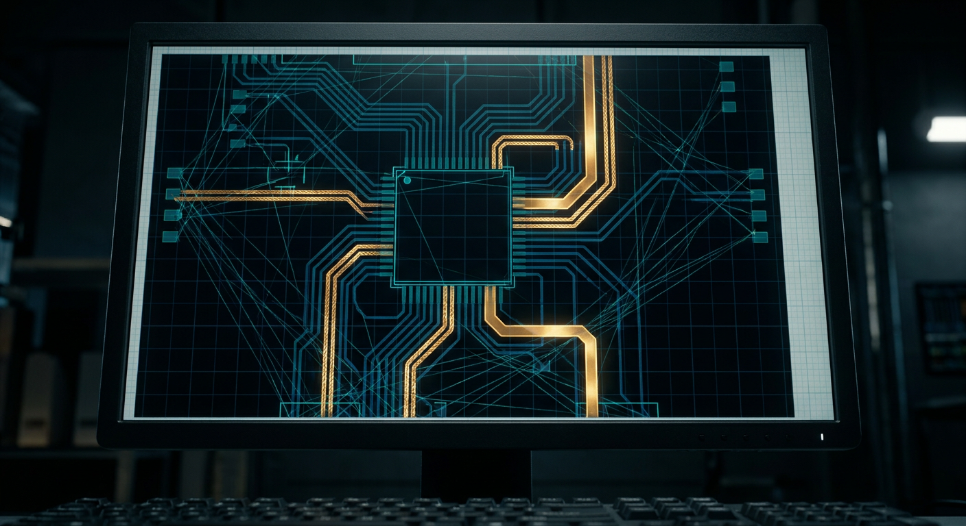
Recent practitioner threads across the EEVblog community and PCB engineering forums have reignited a familiar debate around automated layout engines. When EasyEDA Pro rolled out its cloud autorouter updates and AI-driven layout tools like DeepPCB gained wider visibility, solo hardware engineers tested them on standard mixed-signal microcontrollers. The outcome surprised nobody who has ever troubleshot a prototype in an RF chamber. The automated engines cleared DRC with 100 percent completion rates, yet placed high-current switch nodes directly beneath sensitive analog front ends, routed USB differential pairs across split ground planes, and snaked crystal oscillator traces across the entire length of the top layer.
The resulting boards were electrically continuous in the netlist, but completely broken in physical reality.
For a solo hardware engineer at an early-stage startup or an SME, this failure mode represents a brutal trade-off. Routing a dense six-layer board with an STM32, a cellular modem, power management ICs, and sixty slow GPIOs takes forty to sixty hours of manual mouse clicks. Full-board automated routing takes five minutes, but produces an unmanufacturable board that costs two weeks and thousands of dollars in prototype respins.
The answer is not to abandon automated routing entirely, nor is it to blindly trust push-button AI tools. The most effective approach used by experienced layout practitioners is a structured hybrid routing protocol: manually place and route the critical physics-sensitive traces, freeze or pin those copper paths inside the EDA database, and only then unleash automated routing engines on the non-critical digital interconnects. Here is how to build and execute that workflow without wrecking your signal integrity.
The Failure Modes of Unconstrained Layout Engines
To understand why unconstrained automated routers fail, you must look at how layout algorithms score success. Classical maze-running autorouters and modern reinforcement-learning tools optimize for a simple geometric objective function: connect pin A to pin B with minimum trace length, zero clearance violations, and the fewest possible vias.
Physics does not operate on pure geometric connectivity. In physical electronics, return currents flow through the path of least impedance, switching regulators generate high-frequency magnetic fields proportional to loop area, and high-impedance inputs act as antennas for nearby capacitive cross-talk.
When you give an automated engine free rein across an entire PCB, it systematically creates four distinct hardware bugs.
1. Switch-Node Area Blooming
On a buck or boost converter, the switch node connecting the inductor, switching FET, and catch diode toggles at hundreds of kilohertz or megahertz with sharp rise times. This copper node carries massive dv/dt and di/dt. If an autorouter handles this net, it often routes it through vias to inner layers, widening the loop area and turning the trace into an active dipole antenna. The result is radiated emissions that fail FCC and CE testing, along with capacitive noise injected directly into adjacent signal layers.
2. Crystal Oscillator Tank Corruption
Microcontroller oscillators operate using high-impedance, low-amplitude resonant circuits. The traces between the quartz crystal, load capacitors, and MCU pins must be short, guarded, and isolated from high-speed digital switching. Automated engines treat crystal nets like ordinary 3.3V GPIO lines. They routinely route them parallel to SPI bus lines or punch ground planes beneath them, leading to startup failures, clock jitter, or intermittent MCU resets at elevated temperatures.
3. Differential Pair Discontinuity
Differential pairs like USB 2.0 High Speed, RS-485, or Ethernet require tight intra-pair coupling and consistent reference plane continuity to maintain controlled differential impedance. Standard autorouters frequently split the pair around vias, introduce asymmetrical stubs, or route the positive and negative legs across plane splits. While the netlist shows both lines connected, common-mode noise skyrockets and eye diagrams collapse.
4. Ground Plane Fragmentation
When an automated router attempts to complete the last five percent of dense digital ratlines, it drops vias aggressively across the board. This creates a dense swiss-cheese pattern of antipads in the inner ground reference planes. Return currents from high-speed signals are forced to travel around these via clusters, dramatically increasing loop inductance and causing unexpected ground bounce across logic ICs.
The Three-Tier Constraint Hierarchy
A production-ready layout workflow separates your schematic netlist into three distinct tiers based on physics, current density, and noise sensitivity. You only automate the tier that cannot cause a board respin.
+-------------------------------------------------------------+
| TIER 1: CRITICAL PHYSICS (100% Manual Routing & Pinned)     |
| - Switch-mode power supply (SMPS) power loops and SW nodes  |
| - Crystal oscillator tanks (XTAL_IN / XTAL_OUT)             |
| - Precision analog front-ends (ADC inputs, current shunts)  |
| - High-voltage or high-current isolated domains             |
+-------------------------------------------------------------+
                               |
                               v
+-------------------------------------------------------------+
| TIER 2: CONTROLLED IMPEDANCE (Constrained Auto / Interactive)|
| - Differential pairs (USB, Ethernet, CAN-FD, RS-485)        |
| - Fast single-ended interfaces (SDIO, QSPI, RGMII)          |
| - Length-matched parallel busses (SRAM, camera sensors)     |
+-------------------------------------------------------------+
                               |
                               v
+-------------------------------------------------------------+
| TIER 3: BULK DIGITAL IO (Automated Routing Candidate)        |
| - Low-speed serial lines (I2C, low-baud UART)               |
| - Static GPIOs, status LEDs, and configuration pull-ups     |
| - Reset lines and enable pins with local filtering          |
+-------------------------------------------------------------+
Tier 1: Critical Physics Nets (100% Manual Routing, Zero Automation)
These nets must be placed, routed, and fully verified by human engineering judgment before any automated tool is opened.
- DC-DC Converter High-Current Loops: Minimize the surface loop area between the input decoupling capacitor, high-side FET, low-side switch, inductor, and output capacitor. Keep these traces on the primary component layer without layer transitions where possible.
- Switch Nodes (SW / PH): Route with short, wide copper pours directly between IC pins and the inductor. Keep clearances generous to avoid capacitive coupling into adjacent signals.
- Oscillator Circuits: Keep crystal traces direct, symmetric, and under five millimeters in length. Surround the tank with a local ground keepout or coplanar guard ring tied back to the IC ground pin.
- Analog Measuring Nodes: Current-sense Kelvin connections, thermocouple inputs, and high-impedance voltage dividers must be routed directly to the ADC without sharing copper with digital returns.
Once Tier 1 is routed, every segment, via, and copper pour associated with these nets must have its status set to Locked or Pinned in the EDA database. Pinned tracks cannot be ripped up, nudged, or recalculated by automated tools.
Tier 2: Controlled Impedance and High-Speed Nets
Tier 2 covers high-speed signals where trace geometry, reference planes, and length matching determine signal integrity.
For differential pairs (USB 2.0 D+/D-, CAN, Ethernet), apply explicit Non-Default Rules (NDRs) in your EDA tool. Define the differential trace width, intra-pair gap, and minimum ground clearance based on your specific PCB fabricator stackup (such as standard JLC2313 or Isola 370HR stackups). Use interactive push-and-shove routing with differential pairing mode enabled to route these from source to destination.
Verify that the solid reference ground plane on the adjacent layer is completely unbroken beneath the entire path. Once verified, pin these tracks. Do not let an automated router handle length-tuning meanders or via placement on Tier 2 nets unless the router explicitly supports differential coupling awareness and return-path checking.
Tier 3: Bulk Digital IO (The Automated Zone)
This tier contains thirty to seventy percent of the total pin count on modern microcontrollers: LED indicators, pushbuttons, boot configuration strapping pins, enable lines, relay drive signals, low-speed UART debugging ports, and standard I2C buses.
These signals operate with slow edge rates or low switching frequencies. As long as basic clearance, minimum trace width, and plane integrity rules are maintained, their exact routing path has negligible impact on board operation. This is the exact domain where automated layout engines provide massive leverage to a solo hardware engineer.
Turnaround and Layout Quality Comparison
To evaluate the practical impact of this hybrid strategy against pure manual routing and unconstrained autorouting, consider the following representative composite benchmark. This composite reflects typical engineering outcomes on a four-layer mixed-signal industrial controller board featuring an STM32F4 MCU, a 24V-to-3.3V buck regulator, RS-485 transceiver, USB 2.0 port, and 42 auxiliary digital IO nets.
Note: The figures below represent an illustrative engineering composite based on typical mid-complexity 4-layer microcontroller designs and standard fab turnarounds.
| Layout Strategy | Manual Layout Time | Automated Run Time | Post-Route Cleanup | Initial Prototype Pass Rate | EMC Chamber Outcome | Respin Risk Level |
|---|---|---|---|---|---|---|
| 100% Manual Routing | 36 - 48 hours | 0 min | 2 - 4 hours | 95% | Pass (Standard filtering) | Very Low |
| 100% Unconstrained Auto | 2 - 4 hours (Setup only) | 5 - 15 min | 18 - 24 hours | 35% | High failure (Radiated EMI) | Severe |
| Hybrid Pinning Protocol | 8 - 12 hours | 10 - 20 min | 2 - 3 hours | 92% | Pass (Standard filtering) | Low |
In the unconstrained automated route, the apparent time savings disappear during post-route cleanup or lab debugging. Ripping up hundreds of fragmented tracks to fix a noisy power rail takes longer than routing the board cleanly from scratch.
In contrast, the hybrid protocol yields an 80 percent reduction in manual mouse mileage while preserving the exact physical layout needed for clean power delivery, low noise, and first-pass fabrication success.
The Step-by-Step Pinning Protocol
To execute this hybrid workflow effectively in tools like Altium Designer, KiCad, Cadence OrCAD, or modern AI routing platforms, follow this strict procedural sequence.
+-------------------------------------------------------+
| STEP 1: Component Placement & Power Floorplanning     |
| - Group by functional domain (Power, MCU, Analog, IO) |
| - Orient ICs to shorten high-speed & switch loops     |
+-------------------------------------------------------+
                           |
                           v
+-------------------------------------------------------+
| STEP 2: Route Tier 1 Physics Nets (Manual)            |
| - SMPS power stages, switch nodes, inductors          |
| - Crystal oscillators and load capacitors             |
| - Precision analog, shunts, Kelvin lines              |
+-------------------------------------------------------+
                           |
                           v
+-------------------------------------------------------+
| STEP 3: Route Tier 2 High-Speed Interfaces (Manual)   |
| - Differential pairs, impedance-matched buses         |
| - Check continuous reference planes beneath traces    |
+-------------------------------------------------------+
                           |
                           v
+-------------------------------------------------------+
| STEP 4: Lock/Pin All Completed Geometry               |
| - Select all Tier 1 and Tier 2 tracks, vias, pours    |
| - Set property to 'Locked' or 'Pinned' in EDA DB      |
+-------------------------------------------------------+
                           |
                           v
+-------------------------------------------------------+
| STEP 5: Define Global Autorouter Keepouts             |
| - Place routing keepout boxes over power stage areas  |
| - Place routing keepouts around oscillator tanks      |
| - Restrict autorouter layer budget if necessary       |
+-------------------------------------------------------+
                           |
                           v
+-------------------------------------------------------+
| STEP 6: Execute Automated Routing on Tier 3 Nets      |
| - Let engine solve bulk digital IO connections        |
+-------------------------------------------------------+
                           |
                           v
+-------------------------------------------------------+
| STEP 7: Post-Route Ground Plane & Return Path Audit   |
| - Inspect layer 2/3 ground planes for via clusters    |
| - Add ground stitching vias to eliminate slot loops   |
| - Run final Design Rule Check (DRC)                   |
+-------------------------------------------------------+
1. Component Placement and Power Floorplanning
Do not start routing until your component placement is locked. Group components by functional domains: high-voltage power input, DC-DC regulation, digital core, high-speed interfaces, and field IO. Place bypass capacitors directly adjacent to their corresponding MCU power pins with immediate via connections to the power and ground planes.
2. Manual Execution of Tier 1 and Tier 2 Nets
Route your power supply switching paths with broad polygon pours on the top layer. Keep the return loop on the adjacent layer directly underneath. Route the crystal oscillator traces on the top layer with zero vias. Route differential pairs with proper spacing and termination resistors placed close to the receiver or transceiver pins.
3. Database Locking and Attribute Assignment
Select all routed tracks, vias, and copper polygons associated with your Tier 1 and Tier 2 nets. In your EDA tool:
- In KiCad: Select tracks, right-click, and select Lock (or press
L). - In Altium Designer: Open the Properties panel, filter by selection, and check the Locked checkbox for Primitives.
- In Cadence Allegro: Set the net property to
FIXED.
Ensure that your autorouter configuration settings have the option "Respect Locked/Fixed Objects" explicitly enabled. Most production routers will not touch locked tracks, but verifying this in your rule deck prevents painful surprises.
4. Setting Up Routing Keepouts and Non-Default Rules
Automated engines will happily route a slow 3.3V GPIO line right through the middle of an SMPS inductor footprint or through the space between crystal load capacitors if copper space exists.
Draw formal Routing Keepout Zones across all signal layers over the entire footprint of:
- The DC-DC converter switching area and inductor.
- The crystal oscillator tank and its grounding perimeter.
- Any sensitive analog front-end components.
This forces the automated engine to path non-critical digital IO around these sensitive areas rather than through them.
5. Running the Engine and Layer Allocation
Configure the automated router to operate primarily on designated signal layers (for example, Layer 1 and Layer 4 on a standard four-layer board with solid ground and power planes on Layers 2 and 3).
Set realistic clearance constraints. If your fab house charges extra for 4-mil traces and 0.2mm drill vias, configure your automated router with a 6-mil minimum trace width and 0.3mm drill size. Allowing an autorouter to drop microvias when standard through-hole vias fit easily will unnecessarily inflate your bare-board invoice.
6. Post-Route Ground Plane Audit
Once the automated engine completes the Tier 3 connections, do not immediately export Gerbers. Perform a visual and automated return-path audit.
Look at Layer 2 (your primary ground reference plane). Turn off all other layers except Layer 2 and your via drill holes. Look for areas where the autorouter dropped five or six vias in a tight row. These via antipads merge together in the copper pour, creating a physical slot or trench in the ground plane.
If any signal on an outer layer crosses that slot, the return current cannot travel directly beneath it. Instead, the return current must detour around the entire slot, creating an unintended magnetic loop antenna. Manually space out these via clusters and drop dedicated ground stitching vias nearby to maintain low ground plane impedance.
What This Means for IntelCAD
The industry is shifting away from naive black-box autorouting toward physics-aware layout automation. Production hardware cannot rely on toy routing engines that ignore return currents, thermal dissipation, and component lead times.
At IntelCAD (intelcad.ai), this hybrid reality forms the foundation of our engineering architecture. Instead of treating a printed circuit board as an abstract graph-theory puzzle, IntelCAD operates with full awareness of power loop geometry, signal return paths, and live component availability from distributors like Digi-Key and Mouser. By enforcing constraint hierarchies and pinning critical physical nets automatically during schematic synthesis, modern engineers can cut layout cycle times by eighty percent while ensuring the resulting boards pass real-world EMC and DFM checks on the first fab turn.
Summary Checklist for Solo Engineers
Before running any automated routing tool on your next prototype revision, run through this four-point verification check:
- Are all SMPS switch nodes, inductors, and current loops routed manually with wide copper and zero layer transitions?
- Are crystal oscillator tanks isolated, direct, and protected by routing keepouts across all signal layers?
- Are all high-speed differential pairs manually routed over continuous, unbroken ground reference planes?
- Are all Tier 1 and Tier 2 tracks, pads, and vias explicitly set to Locked/Pinned in your EDA database properties?
If all four answers are yes, turn your automated engine loose on the remaining digital IO. You will save dozens of hours of repetitive layout work without sacrificing board yield, signal integrity, or prototype schedule.
Sources
[1] DeepPCB AI PCB Routing - https://deeppcb.ai/
[2] Reddit PCB Autorouting Practitioner Discussions - https://www.reddit.com/r/PCB/comments/1qygy2c/which_pcb_design_software_is_the_best_for/
[3] LibrePCB Layout & Routing - https://news.ycombinator.com/item?id=37694414
[4] Sierra Circuits: Designing Hybrid PCB Stackups - https://www.protoexpress.com/blog/how-to-design-and-build-a-hybrid-pcb-stackup/
[5] Cadence PCB Design: Stackup and High-Speed Signal Routing - https://community.cadence.com/cadence_technology_forums/pcb-design/f/allegro-x-pcb-editor/64996/hybrid-pcb-stackups-why-they-matter-and-how-to-get-them-right
[6] Siemens Electronic Systems: Fundamentals of Signal Integrity and Critical Nets - https://blogs.sw.siemens.com/electronic-systems-design/2010/04/23/fundamentals-of-signal-integrity-part/
[7] EasyEDA Pro Routing Engine Documentation - https://prodocs.easyeda.com/en/pcb/route-auto-routing/
[8] EEVblog Forum: Autorouter Limitations in Practical Board Manufacturing - https://www.eevblog.com/forum/manufacture/easy-eda-autorouter-fails-miserably/25/