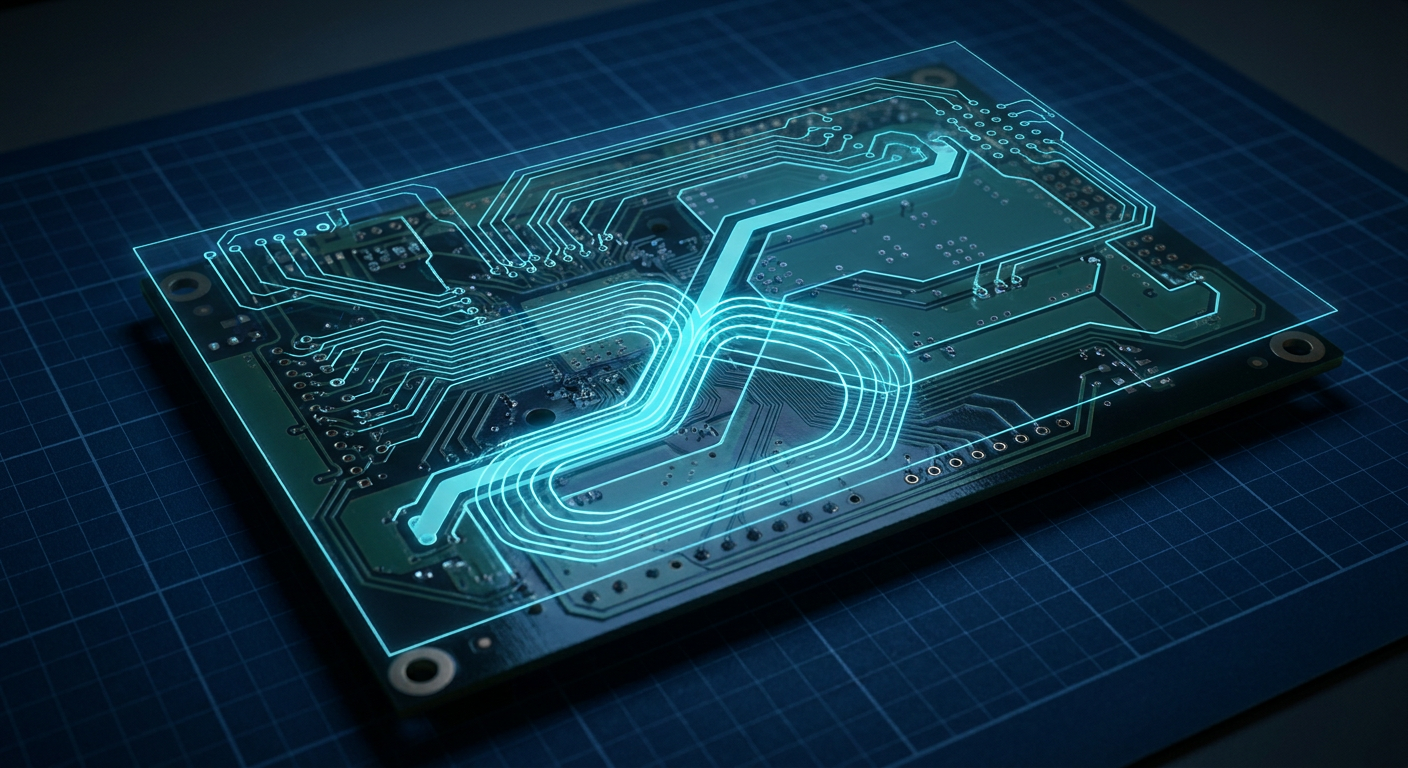
Free web-based design for manufacturability (DFM) checkers and AI-driven CAM tools have become the standard pre-flight gate for hardware startups. Over the past six months, automated services from fabricators like JLCPCB, Sierra Circuits, and Advanced PCB have expanded their automated file analysis to scan uploaded Gerber and ODB++ archives in seconds. They check annular rings, copper clearances, acid traps, solder mask slivers, and drill aspect ratios before an engineer commits hundreds or thousands of dollars to a quick-turn prototype run.
For a solo engineer balancing board layout, firmware, and component sourcing, getting a green checkmark from an automated DFM tool provides immense relief. The platform reports zero design rule violations, confirms trace-to-pad clearances match fab capabilities, and approves the job for production. Two weeks later, the assembled boards land on the bench. The microcontroller boots, power rails read clean on a multimeter, and low-speed UART diagnostics work as expected.
Then the analog front-end turns on, or the board enters an EMC test chamber for radiated emissions pre-compliance. The 16-bit ADC drops to an effective 10.5 bits of resolution. The 120 MHz SPI clock and switching regulator harmonics blow past FCC Part 15 Class B limits by 14 dB.
The layout passed every automated DFM check without a single warning. The failure was not a manufacturing defect. It was an electromagnetic flaw that 2D geometric algorithms cannot see: a return path discontinuity.
The Physics Blind Spot in Automated DFM
Automated DFM engines operate almost entirely on two-dimensional geometric boundary rules. They analyze copper features on discrete Gerber layers as polygons and line segments. If a trace width measures 0.127 mm and the fab constraint is 0.1 mm, the tool passes it. If the clearance between a trace and an adjacent copper polygon exceeds the minimum 0.127 mm threshold, the tool marks the polygon valid.
High-frequency electromagnetic fields do not care about 2D polygon boundaries.
At DC and very low frequencies below 100 kHz, return current follows the path of least resistance. It spreads throughout the entire copper plane, taking a straight line back to the power supply or regulator ground terminal.
Once signal edge rates shorten into the sub-nanosecond territory common in modern microcontrollers, the current switches behavior completely. High-frequency return current follows the path of least inductance. That path is not a straight line across the board. It is the path of minimum loop area, which forces the return current to travel in the reference plane directly underneath the signal trace.
Due to the skin effect, this current does not even travel through the interior of the copper plane. At frequencies above 30 MHz in 1 oz copper (35 microns thick), skin depth drops below 12 microns. The return current travels strictly on the surface of the reference plane directly facing the signal layer.
When a high-speed trace crosses a gap in that reference plane, the return current cannot jump the air gap. It must divert around the obstacle. That diversion instantly creates an inductive loop, alters the characteristic impedance of the trace, and turns a quiet internal layer into an efficient slot antenna.
Automated DFM tools miss this entirely because they check for netlist continuity and physical spacing, not electromagnetic return loops. If Net A is connected from Pin 1 to Pin 2, and Ground is unbroken somewhere on Layer 2, the geometric checker sees zero defects.
+-------------------------------------------------------------------------+
|                   GEOMETRIC DFM VS. RF RETURN REALITY                   |
+-------------------------------------------------------------------------+
| What Automated DFM Checks:                                              |
|   [Trace Layer]       Trace Width: 0.15mm (OK)  Clearance: 0.15mm (OK)  |
|                       -------------------------------------------->     |
|                                                                         |
|   [Plane Layer]       Isolated Ground Shape A     Isolated Ground B     |
|                       [====================]  GAP  [==============]     |
|                       Net Continuity: OK via star tie point at corner   |
|                       Geometric DRC Result: 0 ERRORS / PASSED           |
+-------------------------------------------------------------------------+
| What High-Frequency Physics Experiences:                                |
|   [Trace Layer]       Signal Edge Rate: 1.2 ns (Tr)                     |
|                       -------------------------------------------->     |
|                                              |                          |
|   [EM Field Loop]                            v (Impedance Discontinuity)|
|   [Plane Layer]       Return Current Flow    |   Return Current Flow    |
|                       <---------------------+ |  (Diverts 25mm away)    |
|                                             +--------------------->     |
|                       Inductive Loop Area Created: 38 mm^2              |
|                       Result: Radiated EMI Peak + Ringing on ADC Line   |
+-------------------------------------------------------------------------+
Three Layout Traps That Pass DFM but Kill Hardware
Return path discontinuities rarely happen because an engineer carelessly cut a plane in half. They happen because practical board layout requires compromises, and modern component packaging creates unintended obstacles.
1. The Mixed-Signal Star Ground Split
Application notes for legacy ADCs and precision operational amplifiers frequently instruct designers to separate analog ground (AGND) and digital ground (DGND), connecting them at a single star point near the power supply. While this technique prevented low-frequency ground loops on double-sided boards in the 1990s, applying it to modern high-speed microcontrollers on 4-layer and 6-layer boards is a primary cause of prototype respins.
When a designer cuts the ground plane on Layer 2 into an analog zone and a digital zone, any digital trace crossing that physical cut loses its reference plane. An engineer routes an SPI bus or an I2C clock from the MCU to a digital-to-analog converter across the split. The trace geometry passes every DFM spacing check.
In reality, the return current cannot cross the moat. It must travel all the way around the split to the star ground point, loop through the analog plane, and return to the driver. The resulting loop area introduces tens of nanohenries of parasitic inductance, causing severe signal overshoot, ground bounce on the ADC reference, and massive radiated emissions at clock harmonics.
2. High-Density Via Fields and Overlapping Anti-Pads
As microcontrollers migrate to fine-pitch Quad Flat No-Lead (QFN-48, QFN-64) and Ball Grid Array (BGA) packages, escape routing requires tightly spaced vias. Each via passing through an internal ground or power plane requires an anti-pad clearance to avoid shorting to the copper.
Standard fab DFM rules require an anti-pad diameter roughly 0.2 mm larger than the drill hole. When four or five vias are placed in a row with 0.5 mm or 0.8 mm pitch, their anti-pads overlap.
The copper between the clearance holes disappears. The result is a continuous slot cutout inside the reference plane. If a high-speed data trace on an outer layer runs across this row of vias, it is crossing a void. Automated DFM sees valid drill clearances and unbroken copper around the perimeter of the board, reporting complete net connectivity while the signal return current is blocked by an invisible wall of anti-pads.
3. Layer Transitions Without Ground Stitching Vias
When a high-speed signal must drop from Layer 1 to Layer 4 on a standard 4-layer stackup (Top Signal, Ground, Power, Bottom Signal), its reference plane changes from the Layer 2 Ground plane to the Layer 3 Power plane.
If the power plane is not decoupled to ground right next to that via transition, the return current cannot follow the signal. The return current on Layer 2 must find the nearest decoupling capacitor to jump to Layer 3, or it must travel to the edge of the board where capacitive coupling between the planes allows it to close the loop.
This creates a massive loop area that encompasses the entire section of the board between the signal via and the decoupling capacitor. The automated DFM engine simply verifies that the via meets minimum hole size and annular ring constraints. It has no mechanism to check whether a ground return via sits within 0.5 mm of the signal transition.
+-------------------------------------------------------------------------+
|               MEASURED IMPACT OF RETURN PATH VOIDS                      |
|               (Composite analysis of mixed-signal MCU prototypes)       |
+-------------------------------------------------------------------------+
| Design Parameter            | Solid Reference Plane | Split Plane Moat  |
+-----------------------------+-----------------------+-------------------+
| Characteristic Impedance    | 50.4 Ohms             | 78.2 Ohms (peak)  |
| Signal Rise Time (10-90%)   | 1.15 ns               | 1.82 ns (sluggish)|
| Peak-to-Peak Ringing        | 42 mV                 | 380 mV            |
| Radiated Emissions @ 120MHz | 28.4 dBuV/m (Pass)    | 44.1 dBuV/m (FAIL)|
| ADC Effective Bits (ENOB)   | 15.2 bits             | 11.4 bits         |
| Standard DFM Status         | PASSED                | PASSED            |
+-------------------------------------------------------------------------+
The Cost of Catching Return Errors Post-Fabrication
When a return path discontinuity passes automated DFM and enters production, the economic damage hits during testing and certification rather than fab processing.
For an early-stage startup or a small hardware team, board respins are rarely about the $250 bare-board invoice. They are about the cascade of secondary costs:
- SMT Assembly Run Loss: A prototype assembly run of 10 to 25 boards with complex microcontrollers, precision sensors, and passives typically costs between $1,500 and $4,500 depending on turn time and component sourcing. If the boards suffer from severe ground bounce or unusable ADC noise, those assembled boards are scrap.
- EMC Chamber Time: Commercial test labs charge between $250 and $450 per hour for anechoic chamber time. Failing a radiated emissions pre-scan within the first forty minutes burns the testing budget and requires booking a second session weeks later.
- Firmware Schedule Slippage: When an analog sensor gives erratic readings due to split-plane ground noise, software engineers often spend weeks trying to filter the problem in digital signal processing routines before realizing the hardware layout is physically corrupt.
A single undetected return path cut can easily push a hardware milestone out by six weeks and drain $8,000 in direct lab and component expenses.
How to Audit Return Paths Before Exporting Gerbers
Since standard DRC and fabricator pre-flight tools do not evaluate electromagnetic fields, solo hardware engineers must implement their own verification checks before releasing manufacturing files.
+-------------------------------------------------------------------------+
|            PRE-GERBER RETURN PATH AUDIT WORKFLOW                        |
+-------------------------------------------------------------------------+
| [1. Stackup Verification]                                               |
|   Verify high-speed signal layers are immediately adjacent to solid GND |
|   Avoid 4-layer stackups with signals separated from GND by thick core  |
|                                                                         |
| [2. Visual Void Inspection]                                             |
|   Turn on high-speed net highlights (SPI, Clocks, USB, PWM, Fast I/O)   |
|   Turn on Ground Plane fill layer only (disable all other layers)       |
|   Trace the physical path of each critical net from source to load      |
|   Verify 100% solid copper directly underneath every millimeter         |
|                                                                         |
| [3. Anti-Pad & Via Trench Audit]                                        |
|   Zoom into dense QFN/BGA breakout areas and connector headers          |
|   Check if clearance holes merge into continuous horizontal/vertical cuts|
|   Stagger via patterns if necessary to maintain copper web continuity   |
|                                                                         |
| [4. Layer Transition Stitching]                                         |
|   For every signal via changing reference planes:                       |
|   - If GND-to-GND: Add GND return via within 0.5mm to 1.0mm             |
|   - If GND-to-PWR: Place 0.1uF 0402 ceramic capacitor immediately beside|
+-------------------------------------------------------------------------+
Step 1: Adopt a Solid, Unified Ground Plane
Abandon physical split planes for analog and digital domains on multilayer boards. Instead of cutting the ground plane, use component placement to enforce domain isolation.
Place all analog conditioning circuitry, references, and sensors on one side of the PCB. Place the microcontroller, power supply, and high-speed digital communications on the opposite side. Pour a single, solid, unbroken ground plane across the entire internal layer directly beneath both sections.
Because high-frequency digital return currents strictly follow the paths beneath their specific traces, digital noise will not wander into the analog section as long as digital traces do not physically cross over into the analog layout zone. You get total noise isolation without creating a return path discontinuity.
Step 2: Visual High-Speed Net Shadowing
Modern EDA suites (such as KiCad, Altium, or modern web-native CAD) allow you to highlight specific net classes. Create a net class for all critical signals: crystal oscillators, clocks, SPI buses, switching regulator switch nodes, PWM outputs, and USB data lines.
Highlight that class in high-contrast bright green. Turn off all board layers except for the high-speed signal layer and its adjacent reference ground plane. Manually follow each highlighted trace from the driving IC to the receiving pin. Verify that the copper beneath the trace is completely solid.
If you see a trace crossing an anti-pad gap, a power plane boundary, or a board cutout, reroute the trace. Never let a fast signal fly across a void.
Step 3: Enforce Via Transition Rules
When a critical high-speed signal must transition between outer layers, the layout must provide a path for the return current to transition between reference planes simultaneously.
If the board stackup has ground planes on both Layer 2 and Layer 3 (common in high-performance 6-layer boards), place a ground via immediately adjacent to the signal via. The distance between the signal via and the return via should be kept under 1.0 mm to minimize the parasitic inductance of the loop.
If the signal transitions from a layer referenced to Ground to a layer referenced to a Power plane, place a high-frequency decoupling capacitor (typically 10 nF to 100 nF in an 0402 package) directly between the signal via entry and exit coordinates. The capacitor acts as a high-frequency AC bridge between the two DC voltage potentials, providing a low-impedance path for the return current.
Step 4: Stagger Breakout Vias
In dense breakout areas under fine-pitch microcontrollers, avoid placing vias in perfectly straight rows if their anti-pads touch.
By staggering the via positions in a zig-zag or diagonal pattern, you preserve a continuous web of copper between adjacent clearance holes. This copper web allows the ground plane to remain contiguous, providing a continuous return path for traces escaping the inner rows of the package without requiring additional PCB layers.
The Limit of Automated Pre-Flight Checks
Automated DFM tools will continue to improve, adding basic netlist clearance checks and automated acid trap detection. However, treating a standard DFM approval as a guarantee of circuit functionality is a dangerous assumption for any hardware engineer.
Manufacturing verification engines are built to tell you if a fab house can physically etch, drill, and plate your board without causing a physical short or open circuit. They are not signal integrity engines. They do not simulate return current distribution, calculate loop inductance, or predict common-mode radiated fields.
Until AI-assisted layout engines incorporate real-time 3D electromagnetic field solvers directly into the routing pipeline, the responsibility for verifying return current continuity rests squarely on the designer. Reviewing the solid copper underneath your fastest nets before exporting manufacturing archives remains the highest-ROI ten minutes you can spend in any PCB layout cycle.
What This Means for IntelCAD
Catching return path discontinuities cannot be treated as a disconnected post-processing check after routing is finished. Truly reliable hardware design requires layout tools that understand the physical electromagnetic relationship between trace geometry, layer stackups, and reference planes from the moment autorouting starts.
IntelCAD (intelcad.ai) integrates physics-aware routing constraints directly into its automated layout pipeline. Instead of routing traces based purely on geometric clearances, the engine continuously tracks return current loop areas and reference plane integrity in real time.
When a signal transitions across layers, the system automatically places return stitching vias and prevents traces from routing across split power planes or overlapping via anti-pads. By combining physics-based layout automation with live BOM availability from major distributors, the goal is simple: deliver production-ready boards that pass both the fab house's geometric DFM rules and real-world signal integrity requirements on the very first spin.
Common Questions on Return Path DFM
Why do AI DFM checks miss return path discontinuities?
Automated DFM tools only verify 2D geometric manufacturability constraints, such as minimum trace width, clearance spacing, and drill-to-copper distances. They evaluate electrical connectivity as a simple DC netlist graph without running electromagnetic field simulations. As long as a ground plane has overall DC continuity somewhere on the board, the geometric check passes, completely ignoring high-frequency AC return current loop paths, plane cutouts, and anti-pad slots.
How fast does a signal edge need to be before return path continuity matters?
Return path continuity matters whenever the signal rise or fall time is shorter than roughly three times the propagation delay across the trace. In practical terms, any signal with an edge rate faster than 2 to 3 nanoseconds, which includes modern 3.3V and 1.8V microcontrollers running simple SPI, I2C, PWM, or SDIO lines, behaves as a high-frequency transmission line where return current strictly follows the path of lowest inductance directly beneath the trace.
Should I ever split the ground plane on a mixed-signal microcontroller board?
No. Modern high-speed mixed-signal design practice strongly recommends using a single, solid, unbroken ground plane across the entire board. Rather than creating physical cuts in copper, isolate noisy digital circuits from sensitive analog components through disciplined physical floorplanning. Keep digital traces strictly within the digital region so their return currents never flow through the copper beneath the analog circuitry.
Sources
- ALLPCB Mixed-Signal Layout Guide: https://www.allpcb.com/blog/pcb-design/dfm-pitfalls-to-avoid-in-mixed-signal-pcb-layout.html
- Sierra Circuits Signal Integrity and Current Return Path: https://www.protoexpress.com/blog/current-return-path-signal-integrity/
- Henry Ott Consultants Stackup and Return Path Analysis: https://hott.shielddigitaldesign.com/techtips/pcb-stack-up-6.html
- In-Circuit Design (iCD) Return Path Discontinuities Analysis: https://www.icd.com.au/articles/RPD_PCBD-Apr2017.pdf
- PCBsync Case Study on Uncaught DFM Return Path Failures: https://medium.com/@pcbsync/the-pcb-design-flaw-that-cost-us-187-000-a-return-path-failure-no-dfm-review-caught-8ff5d6069b6e
- EMA Design Automation Return Path Mitigation Strategies: https://www.ema-eda.com/ema-resources/blog/investigating-return-path-discontinuities-understanding-impacts-and-effective-mitigation-strategies/