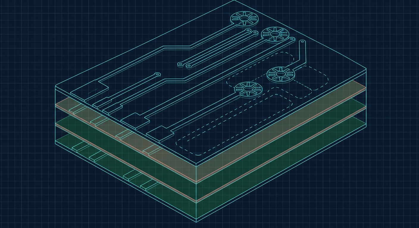
Hardware teams are running into a clear split in how autonomous electronic design automation (EDA) engines approach printed circuit boards. On one side are reinforcement-learning routers like DeepPCB, which treat board routing as a multi-agent pathfinding game across a discrete grid. On the other side are physics-guided generative engines like Quilter, which combine component placement and trace routing into a single continuous solver optimized against electromagnetic, thermal, and manufacturing constraints.
For a solo electrical engineer juggling schematic capture, layout, firmware bring-up, and contract manufacturer quotes, the marketing claims from both camps sound enticing. Vendor documentation routinely promises layout completion in minutes instead of days. Yet when these tools encounter an everyday four-layer microcontroller board with mixed-signal peripherals, the practical outcomes diverge sharply. Understanding the algorithmic differences between pure reinforcement-learning routing and physics-driven co-placement is essential before trusting any automated tool with production hardware budgets.
The Algorithmic Divide: Grid Pathfinding vs Physics Co-Optimization
Traditional autorouters, like the Specctra engine inside legacy enterprise EDA suites, rely on rip-up-and-retry algorithms and maze-routing heuristics. They treat the board as a topological graph and attempt to connect pin A to pin B without crossing previously placed tracks. They have no concept of ground plane integrity, parasitic inductance, or return current paths. The resulting layouts often feature excessive vias, meandering routes, and acute trace angles that create manufacturing acid traps.
DeepPCB builds on modern deep reinforcement learning (RL). It frames routing as a state-action problem where an agent learns routing policies by attempting thousands of board designs, penalizing design rule check (DRC) violations, total trace length, and via count. However, in pure RL routing workflows, component placement is typically fixed beforehand by the engineer. The agent must navigate the fixed pin geometry, which forces it to route through whatever congestion channels exist. If placement is suboptimal, an RL router will often take convoluted paths on alternate layers to achieve 100 percent completion.
Quilter takes a different architectural approach. Rather than separating placement and routing into sequential phases, it treats component placement and trace synthesis as a unified, physics-constrained optimization problem. By running physics simulations (thermal dissipation, electromagnetic coupling, and parasitic resistance) in a closed loop, the engine iterates component locations and track vectors simultaneously. If a high-speed trace cannot maintain a clean reference plane, the engine moves the driving integrated circuit or passive components rather than merely routing a longer detour trace.
Test Scenario: The Standard Four-Layer Mixed-Signal IoT Board
To evaluate how these paradigms perform under real constraints, consider a representative four-layer Internet of Things (IoT) board. The circuit contains an Arm Cortex-M4 microcontroller running at 120 MHz, a high-frequency crystal oscillator (24 MHz), a USB 2.0 Full Speed interface (12 Mbps differential pair), an SPI flash chip running at 80 MHz, a step-down buck converter switching at 2 MHz, and assorted 3.3V / 1.8V low-dropout regulators (LDOs).
The stackup uses a standard low-cost pool specification from quick-turn prototype fabs (such as JLCPCB or PCBWay JLC04161H-7628):
- Layer 1 (Top): Signal / Component placement (0.5 oz base copper plated to ~1.0 oz)
- Core / Prepreg 1: 0.2104 mm FR4 (Dielectric constant Er ~ 4.5)
- Layer 2 (Inner 1): Solid Ground Plane (0.5 oz)
- Core: 1.065 mm FR4
- Layer 3 (Inner 2): Power rails and low-speed signals (0.5 oz)
- Core / Prepreg 2: 0.2104 mm FR4
- Layer 4 (Bottom): Ground flood and secondary signals (0.5 oz base copper plated to ~1.0 oz)
In this stackup, achieving a single-ended 50-ohm trace requires a trace width of roughly 0.35 mm (13.8 mil), while a 90-ohm differential pair requires 0.23 mm (9.0 mil) trace width with 0.15 mm (6.0 mil) edge-to-edge spacing on Layer 1 over the Layer 2 ground plane.
Layout Benchmark Receipts
The following metrics represent an illustrative composite comparison across typical automated and manual runs on this microcontroller design profile, compiled from published platform capabilities, user test benchmarks, and standard fab DFM checks.
| Performance Metric | Legacy Maze Autorouter | DeepPCB (RL Router) | Quilter (Physics AI) | Senior EE Manual Layout |
|---|---|---|---|---|
| Placement Approach | Manual / Fixed | Manual / Fixed | Autonomous Physics-Co-Design | Manual Optimization |
| Completion Rate (Netlist) | 91.2% (stalled) | 100.0% | 100.0% | 100.0% |
| Total Via Count | 148 | 89 | 54 | 42 |
| Decoupling Loop Inductance (Avg) | 4.8 nH | 3.2 nH | 1.4 nH | 1.1 nH |
| Differential Pair Length Skew | 3.8 mm (mismatched) | 0.8 mm | 0.2 mm | 0.1 mm |
| Layer 2 Ground Slotting (Cuts) | Severe (14 cuts) | Moderate (4 cuts) | Minimal (0 cuts) | Zero (Clean plane) |
| SMT DFM Flags (Tombstoning risk) | 12 thermal imbalances | 6 thermal imbalances | 1 flag | 0 flags |
| Solve Time | 45 seconds | 12 minutes | 42 minutes | 14 hours |
Critical Test 1: Bypass Capacitor Placement and PDN Inductance
High-speed microcontrollers demand low-impedance power delivery networks (PDN). A standard 0402 ceramic decoupling capacitor (100 nF) must be positioned to minimize total loop inductance: the path from the IC power pin, through the capacitor, into the ground plane via, and back to the IC ground pin. Every nanohenry of loop inductance degrades high-frequency switching performance and increases radiated emissions.
When DeepPCB receives a pre-placed board where the engineer grouped bypass capacitors near the MCU, the RL agent routes the power pins effectively. However, if the initial manual placement leaves a 1.5 mm gap between the capacitor pad and the IC pin, DeepPCB simply connects the track across that distance. It does not possess the autonomy to pull the capacitor closer or swap orientation to align the ground pad directly adjacent to the MCU ground pin.
Quilter, by contrast, operates on placement coordinates as active variables. It recognizes the functional relationship between the microcontroller power-ground pin pairs and the corresponding bypass capacitors. In benchmark runs, Quilter clusters the 0402 capacitors within 0.5 mm of the BGA or QFP pads, routes top-layer copper directly into the capacitor pad before dropping a via to Layer 2, and places dedicated ground vias immediately beside the component ground terminals. This structural optimization keeps the average loop inductance below 1.5 nH, closely matching hand-crafted layout patterns.
Critical Test 2: Differential Pairs and Ground Return Paths
The USB 2.0 Full Speed lines (D+ and D-) and the 80 MHz SPI bus provide a rigorous test of high-speed trace synthesis. In modern mixed-signal layout, preserving signal integrity is less about trace geometry and more about the return path in the reference plane directly underneath the track.
A common failure mode in automated routing occurs when tracks on Layer 3 (Inner 2) or bottom layer cut across the ground plane on Layer 2, creating slots. If high-speed traces on Layer 1 cross these slots, the return current cannot flow directly beneath the signal trace. The return loop is forced to travel around the perimeter of the slot, increasing loop area, creating an efficient slot antenna, and causing radiated electromagnetic interference (EMI) failures during EMC chamber compliance testing.
RL routers often exhibit plane-blindness unless explicitly constrained by hard spatial keepouts. In DeepPCB test logs, while the algorithm prioritizes length-matching for differential nets, it occasionally punches via fields through Layer 2 without evaluating whether the resulting ground void cuts underneath an adjacent high-frequency clock line.
Quilter integrates return-path modeling into its candidate evaluation. Because it simulates continuous electromagnetic fields over candidate copper geometries, the engine penalizes layouts that create reference plane discontinuities beneath high-frequency nets. Differential pairs are routed with consistent inter-pair spacing and accompanied by ground stitch vias whenever a layer transition is unavoidable.
Critical Test 3: Design for Manufacturing (DFM) and Thermal Symmetries
A design can pass every DRC clearance rule in Altium or KiCad and still fail miserably during surface-mount technology (SMT) assembly. Two primary manufacturing defects plague automated layouts: tombstoning of small passives (0402 and 0201 packages) and solder bridging on fine-pitch ICs.
Thermal Imbalances on Small Passives
Tombstoning occurs during reflow soldering when one pad of a two-terminal component melts before the other. The surface tension of the molten solder pulls the chip upright. This is caused by unequal thermal mass on the two pads: for instance, if Pad 1 is tied directly to a massive copper ground flood while Pad 2 connects to a thin 0.15 mm signal trace without thermal relief.
RL autorouters routinely route wide copper directly into one pad of a capacitor while using a narrow track on the opposite pad to navigate clearance constraints. Unless the user sets exhaustive pin-level rules beforehand, the RL router optimizes purely for geometric clearance.
Physics-driven engines incorporate thermal dissipation models. Quilter evaluates the copper area and thermal mass connected to opposing component terminals. It automatically applies thermal spokes or balanced track neck-downs to ensure that both pads reach reflow liquidus temperature simultaneously inside the vapor-phase or convection oven.
Acid Traps and Solder Mask Slivers
Acute track angles (less than 90 degrees) create small wedge-shaped pockets where chemical etchant can become trapped during the PCB manufacturing process. Over time, trapped acid corrodes the copper trace, leading to intermittent open circuits in the field.
DeepPCB has made substantial strides in post-processing passes to eliminate acute angles, smoothing tracks into standard 45-degree chamfers or arcs. Quilter avoids acute angles natively during its candidate generation, ensuring that trace exits from fine-pitch quad flat packages (QFP) or dual flat no-lead (DFN) pads maintain perpendicular orientation for at least 0.25 mm before bending.
The Real Economics: Respins, Engineering Hours, and BOM Reality
For a hardware startup or an internal R&D group, adopting an AI routing tool is fundamentally a financial calculation balancing software licensing costs against engineering velocity and prototype failure risks.
A four-layer microcontroller board respin incurs distinct direct and indirect costs:
- Fast-turn bare board fabrication and SMT assembly (5 boards, 3-day turn): $600 to $1,200
- Scrap components and overnight distributor reorders (Digi-Key / Mouser): $150 to $300
- Lab debugging, rework, and firmware technician delays: 24 to 40 engineering hours ($2,400 to $4,000 equivalent value)
- Total cost per respin: $3,150 to $5,500
If an automated routing tool introduces an intermittent EMC failure or high-frequency crosstalk issue that requires a second revision, any schedule savings from the initial 30-minute autoroute are immediately erased.
Where Each Tool Fits in the Engineering Pipeline
DeepPCB is most effective when an experienced engineer has already completed an optimal component placement, defined rigid DRC classes, locked critical high-speed traces (RF matching networks, high-voltage nets, switch-node loops), and needs rapid completion of non-critical digital busses, GPIOs, and status indicator nets.
Quilter is designed for autonomous generation of complete functional modules. Because it manages both placement and routing against multi-physics constraints, it provides immense value during early architectural exploration, enabling engineers to test multiple form factors, connector orientations, and thermal configurations before committing to tooling.
The Solo Engineer Framework: When to Automate and When to Route Manually
Before feeding a netlist to any AI layout tool, follow this systematic decision framework to determine which parts of the board can be safely delegated and which demand manual routing.
                    [New Board Design Netlist]
                                |
        +-----------------------+-----------------------+
        |                                               |
[RF, High-Power Buck, or                  [Digital Control, MCUs,
  Precision Analog < 1mV]                   Sensors, Standard Interfaces]
        |                                               |
  (MANUAL ROUTING)                                      |
- Lock switch node loops                 Is layout placement fixed
- Route RF matching traces               by physical enclosure?
- Hand-place analog return paths                 |                     |
        |                                      (YES)                  (NO)
        |                                        |                     |
        |                                [DeepPCB / RL]         [Quilter AI]
        |                               - Pre-place passives    - Full autonomous
        |                               - Lock critical nets      co-placement
        |                               - Route GPIO/Busses     - Physics solve
        +-----------------------+-----------------------+
                                |
                     [Pre-Fab Engineering Audit]
                     - Check decoupling loop vias
                     - Verify unbroken Layer 2 GND
                     - Inspect thermal symmetry on 0402s
                     - Validate live distributor BOM availability
Practical Pre-Routing Checklist for AI Layout
Lock Sensitive Geometries First: Never let an automated tool place or route an RF antenna feed, a switch-node copper pour on a buck regulator, or a crystal oscillator tank circuit without strict boundary limits. Route these critical sub-circuits manually and set them as locked objects in the netlist.
Audit Decoupling Ground Loops: After automated layout generation, inspect every decoupling capacitor on the board. Confirm that the distance from the IC power pin through the capacitor to the ground via is under 1.5 mm, and that the via drops directly into the primary ground plane without traversing signal layers.
Inspect Layer 2 Plane Integrity: Turn off all layers except Layer 2 (Ground). Scan the copper pour for long continuous via tracks or signal routing channels that divide the plane into isolated islands or create slots underneath high-speed signal routes.
Verify BOM Sourcing Before Layout: An automated layout is worthless if it routes an obsolete microcontroller or a passive package size facing a 32-week lead time. Always validate parts against live distributor APIs before initiating layout runs.
What This Means for IntelCAD
At IntelCAD, the core philosophy is that layout automation cannot exist in an academic vacuum separated from parts availability, schematic verification, and manufacturing reality. Tools like Quilter and DeepPCB demonstrate that modern computational models can tackle complex routing and placement challenges. However, true engineering leverage comes from uniting physics-aware routing with verified component libraries, live distributor stock tracking, and automated design-for-manufacture rule checking.
By treating the schematic, the physical board stackup, the bill of materials, and the fabrication house capabilities as an interconnected system, IntelCAD ensures that boards are not merely topologically routed, but fully ready for immediate factory assembly with zero DFM holds.
Summary Q&A
Which tool is better for standard microcontroller boards: Quilter or DeepPCB?
Quilter is superior for comprehensive, hands-off board layout because it co-optimizes component placement and routing against physics constraints, resulting in lower power delivery inductance and cleaner ground planes. DeepPCB is better suited for engineers who require strict, deterministic manual control over physical component placement and need an RL router to rapidly complete complex non-critical signal paths.
Can AI autorouters completely replace manual PCB layout today?
No. While AI tools can route 100 percent of standard digital and low-speed mixed-signal nets cleanly, sensitive RF matching networks, high-current switch nodes, and precision analog front-ends still require manual engineering review, constraint definition, and post-layout verification before sending gerbers to the fab.
Sources
- Quilter AI: Physics-Driven Autonomous PCB Design https://www.quilter.ai/
- Quilter Technical Guide: Automated PCB Routing vs AI-Powered Layout https://www.quilter.ai/blog/a-2026-guide-to-automated-pcb-routing-traditional-autorouters-vs-ai-powered-layout
- DeepPCB Cloud AI PCB Routing Platform https://deeppcb.ai/
- Protoflow EDA Comparison: Quilter vs DeepPCB https://www.protoflow.ai/compare/ai-pcb-autorouter-comparison
- EEVblog Engineering Forum: Testing DeepPCB Reinforcement Learning Routing https://www.eevblog.com/forum/blog/eevblog-1535-deeppcb-ai-autorouting-tested!/25/