Standard pooled four-layer PCB runs remain the fastest and cheapest way to get hardware into a lab. For under fifty dollars, quick-turn board houses will ship five bare boards in three days. But when your edge compute module or camera sensor needs USB 3.0, MIPI CSI-2, or gigabit Ethernet, quoting engineers often tell you to upgrade immediately to a 6-layer or 8-layer board. That recommendation jumps raw fabrication costs by 300 percent and inflates assembly setups on prototype runs.
The pressure to add layers comes from a real problem: classic 1.6 mm four-layer boards have thick outer dielectrics that make standard 50-ohm single-ended and 90-ohm differential traces impractically wide. If you try to route a wide differential pair into a 0.5 mm pitch BGA or a compact USB-C receptacle, the geometry breaks.
You do not always need a 6-layer board. By choosing modern thin-prepreg four-layer pool stackups, using coplanar ground referencing, and tightly managing reference plane transitions, you can achieve clean 90-ohm and 100-ohm transmission lines on standard prototype budgets.
The Dielectric Thickness Trap on Standard 1.6mm Boards
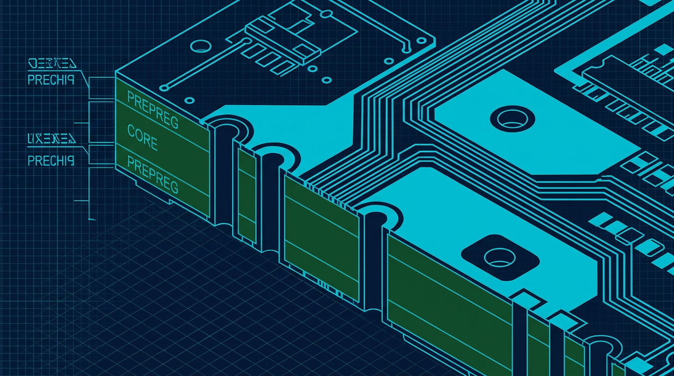
To understand why high-speed signals break on cheap 4-layer boards, you have to look at how fabricators build them. A legacy 1.6 mm four-layer board uses a symmetrical build: a thick prepreg layer on the outside (around 0.2 mm or 8 mils), a thick central core (around 1.0 mm to 1.2 mm), and another thick prepreg layer on the bottom.
Microstrip impedance ($Z_0$) depends primarily on three factors: trace width ($w$), trace thickness ($t$), and the height ($h$) of the dielectric separating the signal trace from the nearest reference ground plane. The characteristic impedance scales inversely with trace width and directly with dielectric thickness:
$$Z_0 \approx \frac{87}{\sqrt{\epsilon_r + 1.41}} \ln\left(\frac{5.98 h}{0.8 w + t}\right)$$
When $h$ is 8 mils (0.2 mm) over standard FR-4 (dielectric constant $\epsilon_r \approx 4.2$ to $4.5$), a single-ended 50-ohm microstrip requires a trace width of roughly 14 to 15 mils (0.38 mm). For a 90-ohm differential pair used in USB 2.0 and USB 3.0, each trace needs to be 11 mils wide with a 6-mil space.
A 14-mil trace cannot escape a 0.5 mm or 0.65 mm pitch camera connector. If you neck the trace down to 4 mils to fit between connector pins without changing the stackup, the local impedance spikes to nearly 85 ohms. That 35-ohm discontinuity creates immediate signal reflections, degrades eye diagrams, and causes intermittent link training failures on high-speed transceivers.
Legacy Balanced 4-Layer (Symmetric):
Layer 1: Signal (1 oz)        ──────────────────
Dielectric 1 (Prepreg):       7.0 - 8.0 mil (Thick -> 14 mil trace for 50Ω)
Layer 2: Ground Plane (1 oz)  ══════════════════
Dielectric 2 (Core):          40.0 - 45.0 mil
Layer 3: Power Plane (1 oz)   ══════════════════
Dielectric 3 (Prepreg):       7.0 - 8.0 mil
Layer 4: Signal (1 oz)        ──────────────────

Modern Asymmetric Fast 4-Layer (Thin-Prepreg Pool):
Layer 1: Signal (1 oz)        ──────────────────
Dielectric 1 (7628/3313/1080): 3.0 - 4.5 mil (Thin -> 5.5 - 7.5 mil trace for 50Ω)
Layer 2: Ground Plane (1 oz)  ══════════════════
Dielectric 2 (Core):          48.0 - 52.0 mil
Layer 3: Power/Ground (1 oz)  ══════════════════
Dielectric 3 (7628/3313/1080): 3.0 - 4.5 mil
Layer 4: Signal (1 oz)        ──────────────────
Select the Right Standard Pooling Stackup
High-volume prototype fabricators now offer pre-engineered controlled impedance stackups inside their standard pricing pools. Instead of using thick outer prepreg, these stackups use thinner glass cloth styles like 7628, 3313, or 1080 between Layer 1 and Layer 2.
Take the standard JLCPCB JLC04161H-7628 and NextPCB 4-layer standard builds as concrete examples. By dropping the outer dielectric thickness down to 3.5 or 4.5 mils (0.09 mm to 0.11 mm), the trace width required for 50-ohm single-ended microstrips drops to 6.0–7.5 mils (0.15–0.19 mm).
For differential pairs, this thin dielectric changes the routing math completely:
4-Layer High-Speed Geometry Comparison
| Interface | Target Differential Impedance | Legacy Thick Prepreg (h = 7.5 mil) | Modern Pool Prepreg (h = 3.6 mil) | Achievable Pitch Fit |
|---|---|---|---|---|
| USB 2.0 / USB 3.x | 90 Ω ± 10% | Trace: 10.5 mil / Space: 6.0 mil | Trace: 5.2 mil / Space: 5.0 mil | Fits 0.65mm BGA & USB-C |
| MIPI CSI-2 / DSI | 100 Ω ± 10% | Trace: 8.5 mil / Space: 6.0 mil | Trace: 4.2 mil / Space: 6.0 mil | Fits 0.5mm FPC connectors |
| PCIe Gen 2/3 | 85 Ω ± 10% | Trace: 12.0 mil / Space: 5.0 mil | Trace: 6.0 mil / Space: 5.0 mil | Fits edge card fingers |
| 1000Base-T Ethernet | 100 Ω ± 10% | Trace: 8.5 mil / Space: 6.0 mil | Trace: 4.2 mil / Space: 6.0 mil | Fits RJ45 magnetic footprint |
Note: Values calculated for finished outer copper thickness of 1.4 mil (1 oz finished over foil), solder mask thickness of 0.6 mil, and FR-4 core dielectric constant $\epsilon_r = 4.2$. Composite data compiled from JLCPCB and NextPCB standard impedance service charts.
When ordering, you must explicitly select the fabricator's designated impedance-controlled stackup code rather than the generic "standard 4-layer" option. Selecting the specific stackup locks the prepreg glass weave and core thickness during panelization, preventing the factory from swapping in random core drops that alter your trace impedance.
Coplanar Waveguides: Routing Differential Signals on Layer 4
In a four-layer board, Layer 2 is almost always assigned as your primary ground plane. This gives top-layer traces (Layer 1) an unbroken, immediate return path just 3.6 mils below.
Layer 4 is more complicated. Layer 3 is typically allocated to power rails (3.3V, 5V, VDD_SOC) or split power islands. If you route high-speed signals on Layer 4 directly beneath a split power plane on Layer 3, the return current is forced to jump across splits. That discontinuity creates massive common-mode radiation and destroys edge rates.
If you must route high-speed pairs on Layer 4 without making Layer 3 a dedicated ground plane, use a Grounded Coplanar Waveguide (CPW-G) layout.
Coplanar Waveguide with Ground (Layer 4 Cross-Section):

     Top Ground Fill        Trace A    Trace B        Top Ground Fill
   ████████████████         ██████     ██████         ████████████████
   ─────────────────────────┬─────┬────┬─────┬─────────┬──────────────
   Dielectric (h = 3.6 mil) │  w  │ s  │  w  │    g    │
   ═════════════════════════╧═════╧════╧═════╧═════════╧══════════════
   Layer 3 Reference Plane (GND or Stable Power)
In a coplanar structure, you flood copper ground on the same layer as your signal traces and bring it close to the pair. The capacitance between the trace edges and the adjacent side ground ($g$) pulls down the overall characteristic impedance. This side coupling allows you to use slightly narrower traces to achieve 90 or 100 ohms while maintaining predictable field lines even if the reference plane beneath is slightly degraded.
Keep these three rules for coplanar routing on outer layers:
- Maintain consistent side ground spacing ($g$): Keep the side ground clearance exactly three times the dielectric height ($g \ge 3h$) unless you intentionally include side coupling in your field solver calculations. If $g < 2h$, the coplanar ground dominates the impedance equation, requiring narrower traces.
- Stitch side ground copper aggressively: Place ground stitching vias along the side ground flood within $\lambda/10$ of your highest frequency harmonic. For a 5 Gbps USB 3.0 signal (fundamental frequency of 2.5 GHz, with significant harmonics up to 7.5 GHz), place ground vias no further than 3 mm apart.
- Do not leave isolated copper slivers: If the ground pour between two differential pairs narrows to less than 15 mils, delete the copper sliver entirely. Floating or poorly stitched copper acts as a patch antenna rather than a shield.
The Three Fatal Mistakes on Budget 4-Layer High-Speed Layouts
Even with the correct stackup and trace width calculations, layout missteps will cause signal integrity failures. On a four-layer board, margin is minimal. You do not have extra internal ground layers to isolate bad decisions.
1. Crossing Reference Plane Splits
A high-speed signal does not travel exclusively inside the copper trace; it travels as an electromagnetic wave in the dielectric between the trace and its return path. The return current flows on the copper surface directly beneath the signal trace, following the path of lowest inductance.
If a 480 Mbps USB 2.0 or 1.5 Gbps MIPI pair crosses a gap in the Layer 2 ground plane, the return current cannot follow. It must detour around the void. This detour expands the current loop area by orders of magnitude, increasing trace inductance, distorting signal edges, and generating severe electromagnetic emissions that will fail FCC or CE testing.
The rule: Keep Layer 2 as 100 percent solid ground across the entire area where high-speed traces run on Layer 1. Never cut Layer 2 with power routing or random signal drop-throughs.
2. Unbalanced Layer Transitions and Missing Stitching Vias
When a differential pair drops from Layer 1 to Layer 4 through vias, its reference plane changes from Layer 2 (Ground) to Layer 3 (Power or Ground).
If Layer 3 is ground, you must place a ground stitching via within 25 mils (0.6 mm) of the signal via pair. This gives the return current an immediate, vertical path to hop between layers alongside the signal.
If Layer 3 is a power plane, the return current cannot hop through a ground via. It must use a 0.1 µF or 10 nF ceramic stitching capacitor placed right next to the signal vias to bridge the ground plane and power plane at high frequencies. If you omit both, the return current will find its own path through the nearest power supply decoupling capacitor inches away, creating substantial cross-talk and jitter.
Signal Layer Transition with Ground Stitching Via:

Layer 1 (Signal Top)     ──[Signal In]──●                     ●──[Signal In]
                                        │ (Signal Via)        │
Layer 2 (Ground Plane)   ═══════════════╪═══════●═════════════╪════════════
                                        │       │ (GND Via)   │
Layer 3 (Ground Plane)   ═══════════════╪═══════●═════════════╪════════════
                                        │                     │
Layer 4 (Signal Bottom)  ──[Signal Out]─●                     ●──[Signal Out]
3. Length Mismatch and Skew Accumulation
Differential signaling relies on the receiver measuring the voltage difference between the positive ($D+$) and negative ($D-$) nets. If the two lines are not matched in physical length, the signals arrive at different times. This timing skew turns differential-mode signals into common-mode noise.
For USB 2.0 High Speed (480 Mbps), intra-pair skew should stay below 50 picoseconds (roughly 7.5 mm of trace length difference in FR-4). For USB 3.0 Gen 1 (5 Gbps) and MIPI CSI-2 (up to 2.5 Gbps per lane), the tolerance is tight: keep intra-pair skew under 5 picoseconds, which equals roughly 0.75 mm (30 mils) of physical length difference.
Add accordion or serpentine tuning patterns immediately adjacent to the source of the length mismatch, such as right after an asymmetrical connector breakout or a bend. Do not wait until the end of the trace to correct skew; running an unmatched differential pair over long distances generates radiated emissions along the entire length of the run.
Practical Verification and Pre-Fab Checklist
Before you push your design files to standard pooling fabrication, run through this step-by-step checklist inside your EDA tool:
- Confirm exact prepreg parameters with the fabricator: Verify the factory stackup name (such as JLC04161H-7628 or equivalent standard build). Check their published dielectric thickness ($h$) and dielectric constant ($\epsilon_r$) at your signal frequency.
- Set up net classes with precise physical rules: Create dedicated net classes for 90-ohm and 100-ohm nets. Lock the calculated trace widths, differential pair gaps, and clearance constraints directly into your design rules.
- Audit Layer 2 for copper voids: Turn off all layers except Layer 1 and Layer 2. Walk the entire length of your high-speed differential pairs. Confirm that a solid, unbroken ground pour exists directly underneath every millimeter of high-speed routing.
- Check length matching reports: Verify that intra-pair length differences for USB 3.0 and MIPI lanes do not exceed 0.5 mm. Check inter-lane skew on MIPI clock-to-data pairs to keep it under 1.5 mm.
- Inspect connector breakouts: Minimize the distance where differential traces uncouple to enter connector pins. Keep uncoupled trace lengths below 3 mm.
- Place ESD protection diodes correctly: Position your TVS diode arrays directly in the path between the connector pins and the series termination resistors or SoC inputs. Never route a high-speed signal past a TVS diode into a stub. The trace must run into the TVS pad and out the other side directly.
What this means for IntelCAD
Designing high-speed interfaces on tight prototype budgets requires connecting physics calculations directly to manufacturing constraints. A layout tool should not let you route a 5 Gbps differential pair over a split plane and pass design rule checks simply because copper clearances are satisfied.
IntelCAD is built around physics-aware layout and real manufacturing stackup profiles. By linking routing engines to fabricator layer pool specifications and live supplier component footprints, IntelCAD ensures that trace geometry, return paths, and BOM components match from schematic capture through physical placement. This eliminates the manual recalculations and hidden signal integrity flaws that turn affordable prototype runs into expensive respins.
Direct Answer: Can You Safely Route High-Speed Signals on a 4-Layer Board?
Yes. You can reliably route USB 3.0, MIPI CSI-2, and Gigabit Ethernet on a 4-layer PCB provided you select a thin-prepreg pooling stackup ($h \le 4.5\text{ mil}$), keep Layer 2 as a solid ground plane directly beneath all signal routes, match intra-pair trace lengths to within 0.5 mm, and place ground stitching vias at every layer transition. If routing on Layer 4, use coplanar ground shielding with stitched vias to guarantee controlled impedance.
Sources
- AdvancedPCB 4-Layer Stackup and Controlled Impedance Guidelines: https://www.advancedpcb.com/en-us/resources/blog/understanding-4-layer-pcb-benefits-designs/
- Altium Technical Documentation on 4-Layer 50-Ohm and 90-Ohm Microstrip Design: https://resources.altium.com/p/two-alternative-4-layer-pcb-stackups-50-ohms-impedance
- JLCPCB Controlled Impedance Stackup Specifications: https://jlcpcb.com/impedance
- NextPCB 4-Layer PCB Stackup and Impedance Control Analysis: https://www.nextpcb.com/blog/4-layer-pcb-stackup-and-impedance-control
- Sierra Circuits Multi-Layer Board Controlled Impedance Guidelines: https://sierraconnect.protoexpress.com/t/impedance-control-in-multi-layer-board-stack-up/2690