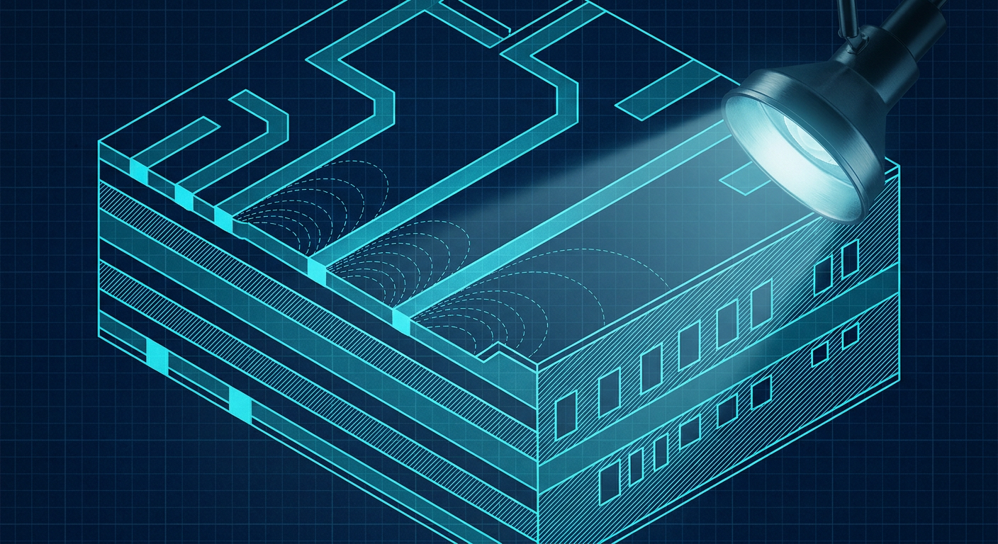
Recent platform updates across cloud autorouting tools like Quilter and DeepPCB emphasize automated design-rule resolution, yet prototype assembly floors continue to see signal integrity failures on high-speed traces that passed automated layout checks. The culprit is rarely a gross layout blunder like an unrouted net or a clear spacing violation. Instead, the failure happens in the invisible layer between the routing engine and the laminate press.
Most cloud autorouters and CAD calculators calculate trace geometries against a flat, idealized relative dielectric constant (Dk) of 4.2 to 4.5 and a static dielectric thickness. Quick-turn fabricators like PCBWay, JLCPCB, and Sierra Circuits do not build boards out of uniform plastic blocks. They use combinations of cured laminate cores and semi-cured prepreg glass weaves (such as 1080, 2116, and 7628 glass styles) that compress, flow, and consolidate under heat and pressure. When the semi-cured epoxy flows into the voids between etched copper features, the final dielectric height drops. That changes the capacitance to the reference plane. Trace impedance shifts by 10 to 15 percent, corrupting single-ended 50-ohm RF feeds and 90-ohm USB differential pairs before the boards even land on the test bench.
For a solo hardware engineer or a lean startup engineering team, this mismatch creates an expensive failure mode. The digital design rule check (DRC) shows zero errors. The autorouter marks the layout 100 percent complete. The assembled prototypes power up, but USB 2.0 High-Speed ports fail handshakes intermittently, DDR lines exhibit eye closure, or BLE front-ends drop range. Tracking down subtle impedance mismatches takes days with a high-bandwidth time-domain reflectometer (TDR) or vector network analyzer. It often leads straight to a board respin that burns two weeks of runway and thousands of dollars in assembly setup fees.
The Physics of the Laminate Press
To understand why algorithmic routing breaks down, look at what happens inside the fabrication press. A multilayer printed circuit board is not a homogeneous structure. It is an alternating stack of pre-cured core laminates (copper clad on both sides with cured C-stage epoxy) and bonding sheets of prepreg (B-stage glass fabric impregnated with partially cured epoxy resin).
When the fabricator places the layer sandwich into a vacuum lamination press and raises the temperature past 170 degrees Celsius, the resin in the prepreg melts into a liquid state. The press exerts hydraulic pressure to drive the liquid resin into the spaces between the copper traces on the adjacent layers. Once the voids are filled, the resin cures into a solid structure.
This physical process introduces two variables that software models frequently ignore:
- Pressed thickness variation. A sheet of 2116 prepreg might have an unpressed nominal thickness of 5.4 mils (0.137 mm). If the adjacent layer has a dense copper ground plane with 85 percent copper coverage, the prepreg does not lose much resin to void filling, settling at roughly 5.0 mils. If that same layer has sparse signal traces with only 15 percent copper coverage, excess resin flows outward, and the pressed thickness over the traces drops to 4.3 mils.
- Effective dielectric constant shifts. Pure epoxy resin has a Dk near 3.2 to 3.5, while woven E-glass fiber has a Dk around 6.0 to 6.5. High-resin prepregs (like 1080, which has roughly 65 percent resin content) have a lower overall Dk of around 3.8. Low-resin prepregs (like 7628, with 45 percent resin content) have a higher Dk around 4.6. When resin flows away from traces to fill surrounding gaps, the local ratio of glass to resin directly under your signal line changes, shifting the local Dk.
When a cloud autorouter assigns a fixed 6.5 mil width for a 50-ohm microstrip using an assumed global Dk of 4.3 and an assumed thickness of 4.0 mils, it operates on a fictional substrate. If the fab presses that dielectric down to 3.2 mils because of low adjacent copper density, the capacitance per unit length increases sharply. The real characteristic impedance drops to 43 ohms. For high-speed buses with tight reflection budgets, that seven-ohm drop is enough to cause severe transmission line reflections.
How Dielectric Variations Degrade Common Interfaces
High-speed transmission lines rely on steady characteristic impedance to prevent signal reflections. When a signal travelling down a trace encounters an impedance discontinuity, a portion of the signal energy reflects toward the driver. The reflection coefficient depends directly on the difference between the source impedance and the instantaneous line impedance.
Single-Ended 50-Ohm Lines (RF and Fast Clocks)
Single-ended 50-ohm microstrips are the standard for sub-GHz radios, Wi-Fi paths, clock distribution networks, and single-ended high-speed digital buses. The characteristic impedance of a surface microstrip is governed primarily by the trace width, the copper thickness, the dielectric thickness to the first reference plane, and the relative permittivity of the material.
Because impedance is inversely proportional to capacitance, and capacitance is inversely proportional to dielectric height, any reduction in pressed dielectric thickness causes impedance to drop. If your CAD tool calculates a 50-ohm trace based on nominal 4.5-mil dielectric spacing, but the fab produces a 3.8-mil spacing after lamination, the trace impedance falls to roughly 44 ohms. For an RF antenna feed line, this creates a voltage standing wave ratio (VSWR) mismatch that wastes transmitter power and degrades receiver sensitivity.
Differential 90-Ohm Lines (USB 2.0 / USB 3.x)
Differential routing adds another layer of complexity. The differential impedance depends not only on the height above the reference ground plane, but also on the edge-to-edge spacing between the two paired traces and the dielectric constant of the material filling the gap between them.
On external layers, the medium between the two traces is a mix of air, solder mask, and the underlying prepreg. Solder mask typically has a Dk between 3.3 and 3.8 and applies unevenly over tight trace spaces. When an autorouter sets trace width and gap based on an unverified stackup, variations in both prepreg compression and solder mask thickness compound each other. A nominal 90-ohm USB pair can shift to 78 ohms or 102 ohms. In USB 2.0 High-Speed (480 Mbps) links, this mismatch causes rise-time degradation and eye mask violations during compliance testing.
The Real-World Discrepancy: A Concrete Comparison
To show how far nominal software defaults drift from physical manufacturing realities, consider a standard four-layer standard-pooling stackup (Layer 1 Signal, Layer 2 Ground, Layer 3 Power, Layer 4 Signal) using 1 oz outer copper and 0.5 oz inner copper.
The following table presents an illustrative composite calculation comparing generic CAD tool default assumptions against actual post-press fabrication parameters measured across common commercial quick-turn pool services (e.g., standard JLC04161H or PCBWay standard 4-layer structures).
| Interface Type | Target Nominal Impedance | CAD Engine Default Assumptions | Resulting Physical Fab Stackup | Actual Physical Impedance | Impedance Deviation |
|---|---|---|---|---|---|
| Microstrip RF | 50.0 Ω | Dk: 4.5, H: 4.5 mil, W: 7.8 mil, T: 1.4 mil | Dk: 4.05 (2116 PP), H: 3.8 mil, W: 7.8 mil, T: 1.2 mil | 43.6 Ω | -12.8% |
| USB 2.0 Diff | 90.0 Ω | Dk: 4.5, H: 4.5 mil, W: 6.0 mil, S: 6.0 mil | Dk: 4.10, H: 4.0 mil, W: 5.8 mil, S: 6.2 mil (Etch factor) | 99.4 Ω | +10.4% |
| Fast Single-Ended | 50.0 Ω | Dk: 4.2, H: 5.0 mil, W: 9.2 mil, T: 1.4 mil | Dk: 4.35 (7628 PP), H: 4.4 mil, W: 9.0 mil, T: 1.3 mil | 45.1 Ω | -9.8% |
| Ethernet Diff | 100.0 Ω | Dk: 4.5, H: 4.5 mil, W: 5.0 mil, S: 7.0 mil | Dk: 4.15, H: 3.9 mil, W: 4.8 mil, S: 7.2 mil | 108.2 Ω | +8.2% |
Notice the pattern. In every case, relying on generic software constants pushes the impedance variation near or beyond the industry standard 10 percent tolerance window. If your fabrication partner works with a standard +/- 10 percent manufacturing tolerance on their own processes, stacking that manufacturing tolerance on top of an uncalibrated design model creates real-world deviations exceeding 20 percent.
Why AI Autorouters Rely on Idealized Models
AI-driven autorouters and cloud layout engines work by solving massive geometric constraint satisfaction problems. To complete thousands of net routes within a reasonable compute budget, their internal physics approximations simplify the continuous field mathematics of electromagnetic propagation.
Most algorithmic tools treat the PCB substrate as a set of flat design rules: minimum trace width, minimum clearance, layer assignments, and target differential spacing. When you request an impedance-controlled net in standard cloud tools, the software usually evaluates a two-dimensional closed-form equation (like standard IPC-2141 microstrip formulas) using a single global Dk value assigned to the whole board.
This simplification fails because:
- Closed-form approximations lose accuracy at small geometries. Empirical equations break down when the trace width is smaller than the dielectric height, or when differential trace coupling interacts strongly with inhomogeneous solder mask coatings.
- Local copper density is ignored. Software engines calculate trace geometries without knowing how much copper will remain on the surrounding signal and plane layers after routing is complete. They cannot anticipate how much resin will squeeze out of the prepreg during lamination.
- Fab-specific prepreg selections are abstracted away. Different fabricators build four-layer and six-layer boards using completely different glass styles. One shop might achieve a 0.1 mm dielectric height using two sheets of 106 prepreg; another might use a single sheet of 2116. While their physical heights may look similar on paper, their resin contents, anisotropic Dk values, and pressed behaviors are distinct.
When you let an automated router generate hundreds of high-speed connections across an idealized substrate, it optimizes purely for geometric rule clearance, not physical transmission line fidelity.
The Pre-Routing Stackup Workflow
To run automated routing tools without risking high-speed signal failure, you must invert the typical workflow. Instead of drawing schematics, autorouting traces, and then picking a fab house, you must lock in the physical fabrication stackup before letting the autorouter touch a single net.
+-------------------------------------------------------------+
| 1. Select Target Fab House & Manufacturing Capability Tier  |
+-------------------------------------------------------------+
                               |
                               v
+-------------------------------------------------------------+
| 2. Pull Exact Tooling Stackup (Laminate Cores + Prepreg)    |
+-------------------------------------------------------------+
                               |
                               v
+-------------------------------------------------------------+
| 3. Run Field-Solver Calculations on True Pressed Geometry   |
+-------------------------------------------------------------+
                               |
                               v
+-------------------------------------------------------------+
| 4. Lock Derived Trace/Gap Rules into Autorouter Constraints |
+-------------------------------------------------------------+
                               |
                               v
+-------------------------------------------------------------+
| 5. Execute Autorouting Engine with Fixed Physical Geometry  |
+-------------------------------------------------------------+
Here is the step-by-step checklist to execute before launching any automated layout run.
Step 1: Identify Your Specific Pooling Tier and Fab House
Quick-turn prototype fabricators publish standard multi-layer laminated structures directly on their websites. For example, PCBWay maintains nearly 300 predefined stackups covering 4-layer to 18-layer configurations, specifying the exact core thicknesses, copper weights, and prepreg types (such as 1080 at 3.1 mil, 3313 at 4.2 mil, or 7628 at 7.7 mil). Choose the exact stackup you intend to order, noting whether it uses standard FR4 (Dk ~4.2 to 4.5) or a higher-performance laminate like Shengyi S1000-2M or Isola 370HR.
Step 2: Use Fabricator-Provided Field Solvers
Do not rely on generic online calculators or the basic default sliders inside your CAD package. Most tier-one fab houses provide integrated impedance calculation tools on their ordering portals that take their proprietary post-press dielectric thicknesses, resin flow allowances, and copper etch-back factors into account. Use their solver to derive the required trace widths and differential spacings for your target impedances (50 ohms single-ended, 90 ohms USB, 100 ohms Ethernet).
Step 3: Account for Solder Mask Thickness
Solder mask adds a thin, high-capacitance layer over surface microstrips that lowers characteristic impedance by 2 to 3 ohms compared to an unmasked line. Ensure your solver includes solder mask parameters (typically 0.8 mil to 1.2 mil thickness over base laminate, with a Dk between 3.3 and 3.6).
Step 4: Inject Solved Geometries as Strict Autorouter Rules
Once you have the fab-verified trace width and gap numbers, hard-code them into your autorouter net class rules:
- Assign your 50-ohm nets to a specific class with a fixed trace width (e.g., 6.8 mils) and restrict them to layers with verified reference planes.
- Assign differential pairs with explicit width, spacing, and intra-pair length matching tolerances.
- Lock these net classes so the automated engine cannot narrow traces to squeeze between dense component pins or via breakouts without throwing a hard DRC violation.
Step 5: Add Copper Thieving and Balance Plane Density
Because prepreg compression depends on copper distribution, unbalanced copper density across your board causes local dielectric height variations. Add solid ground copper pours on unused board areas on all layers, or instruct your fabricator to add automated copper thieving (non-functional copper hatching) in empty zones. This maintains uniform pressure during lamination and ensures the pressed prepreg height matches the nominal datasheet values.
What This Means for IntelCAD
Modern electronics development cannot afford a disconnect between automated layout algorithms and assembly floor realities. IntelCAD integrates physics-aware layout and live supply chain validation directly into the design pipeline. Instead of relying on generic dielectric assumptions, automated tools must ground their placement and routing decisions in verified manufacturing stackups, real DFM parameters, and live distributor component footprints. Treating physical fabrication realities as fundamental inputs rather than downstream afterthoughts is what separates prototype experiments from production-ready hardware.
Practical Rules for High-Speed Layout Safety
When designing boards with controlled impedance, use this practical decision checklist before running any automated layout tool:
- Never use the CAD tool default FR4 Dk. Set the material properties based on the actual laminate datasheet provided by the fabricator for your specific board thickness.
- Verify outer layer copper plating thickness. Outer layers specified as 1 oz copper typically start as 0.5 oz base foil and gain another 0.5 oz to 0.8 oz through electroplating in the via barrels. Ensure your impedance calculator models the final plated copper thickness (typically 1.4 mils) rather than base foil thickness.
- Isolate fast signals from split reference planes. Ensure the layer stackup places high-speed traces over solid, unbroken ground planes. A 50-ohm microstrip crossing a split power plane loses its reference, spikes in impedance, and creates massive EMI problems regardless of stackup accuracy.
- Order standard controlled impedance service when margins are tight. If your design contains buses with less than 10 percent margin (such as DDR4 or PCIe Gen3+), specify fabricator-controlled impedance on your purchase order. The fab will adjust trace etch compensation dynamically and test test-coupons on the production panel with a TDR to verify the impedance within +/- 10 percent or +/- 5 percent before shipping.
By feeding verified, fab-specific dielectric data into your design rules before starting the autorouting engine, you close the gap between software layout models and the physical laminate press. That ensures your automated designs function on the first spin.
Why Do Real-World Stackups Break Default Impedance Models?
Cloud autorouters and CAD calculators assume flat, uniform FR4 dielectric values and static thicknesses. Real PCB fabs use semi-cured prepreg sheets that melt, flow into copper voids, and compress during lamination. This physical resin flow reduces dielectric thickness and alters the local glass-to-resin ratio, shifting trace impedance by 10 to 15 percent away from idealized simulation models.
Sources
- Design for Manufacturability (DFM) in Electronics
- Quilter AI Automated PCB Routing Guide
- The Impact of Layer Stackup on Impedance Control in Multilayer PCBs
- Why PCB Impedance Varies Even With a Defined Stackup
- How to Control your Controlled Impedance - Sierra Circuits
- The #1 Mistake in PCB Impedance Control: Ignoring the Stackup
- Multi-layer Laminated Structure and Prepreg Parameters - PCBWay
- PCB Stackup Design Guidelines - EMA Design Automation