Over the past few months, benchmarking releases from automated layout platforms such as Quilter and DeepPCB have renewed the pitch that autonomous PCB routing is ready for complex boards. The demonstrations are compelling on the surface. You feed an unrouted board file and a netlist into a cloud worker, and within ten to twenty minutes you get back a 100 percent completed layout with zero geometric Design Rule Check (DRC) errors.
For a solo hardware engineer at an early-stage robotics or IoT startup, that kind of turnaround looks like an immediate week of schedule savings. You bypass the tedious fanout of microcontrollers, differential routing of sensors, and power polygon pours.
Then the prototype arrives from the assembly house.
The board boots, but the USB 3.2 Gen 1 interface drops packets at 5 Gbps. The external DDR4 memory bus exhibits random bit flips during burst writes. Radiated emissions testing in the pre-compliance chamber fails standard CISPR 32 Class B limits by 14 dB at 480 MHz.
When you open the layout and turn off the signal layers to inspect the internal reference planes, the culprit is obvious. The autorouter achieved 100 percent trace connectivity by routing high-speed traces directly over split power planes, slotting ground copper with clustered via antipads, and hopping signal layers without placing a single ground stitching via.
The tool satisfied every geometric rule in the design constraints. It completely failed the high-frequency physics of electromagnetic return paths.
The Fundamental Flaw of Geometric and RL Pathfinding
To understand why modern AI autorouters make these mistakes, you have to look at the mathematical objective functions they optimize.
Traditional maze routers based on Lee algorithms or rip-up-and-retry heuristics treat PCB layout as a grid-based topological pathfinding problem. Modern tools powered by reinforcement learning (RL) or spatial optimization engines view layout as a multi-agent resource allocation challenge. The system is rewarded for minimizing total trace length, minimizing via count, and clearing clearance boundaries set by the trace-to-trace DRC rules.
None of those rewards account for how high-frequency currents actually return to their source.
At direct current (DC) and low frequencies below roughly 100 kHz, current follows the path of least resistance. It takes the shortest, widest physical path of copper back to the power supply or ground terminal.
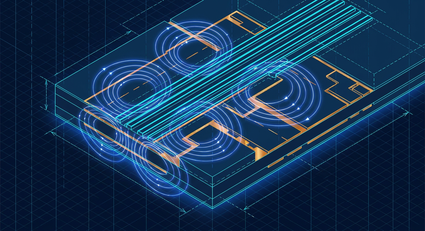
At high frequencies (signals with fast rise times below 1 nanosecond, typical of USB, PCIe, Ethernet, or SPI with steep edges), current follows the path of least inductance. Inductance is determined by loop area. To minimize the loop area formed by the outgoing signal and returning current, the return current gathers in the copper plane directly beneath the signal trace.
The return current density distribution beneath a microstrip trace follows a Lorentzian function:
$$J(x) = \frac{I_0}{\pi h \left(1 + \left(\frac{x}{h}\right)^2\right)}$$
Where $h$ is the dielectric height between the trace and the reference plane, and $x$ is the horizontal distance from the trace centerline. When the dielectric height is 4 mils (0.1 mm), roughly 80 percent of the entire return current is concentrated in a strip just 12 mils wide directly beneath the trace.
If an automated routing agent does not calculate this electromagnetic field profile at every step, it treats copper planes as passive equipotential sheets rather than active transmission line components. The router sees an open 2D coordinate space and routes a trace across whatever layer is clear. It treats a solid ground plane, a fragmented 3.3V power polygon, and empty board space identically, as long as no clearance rule is triggered.
Three Failure Modes Ruining Fast Digital Layouts
When an AI autorouter runs without field-aware return path constraints, it routinely introduces three fatal layout flaws on standard 4-layer and 6-layer boards.
1. Split Plane Traversals and Void Crossing
In dense mixed-signal designs, internal layers often contain split planes for various voltage rails (for instance, 1.8V for an MCU core, 3.3V for legacy peripherals, and 5V for system power). When an AI router needs to take a pair of high-speed differential traces from one IC to a connector, it searches for geometric routing channels.
If the top layer is blocked, it routes on Layer 1 over a split where the Layer 2 ground plane transitions into a 3.3V plane. The trace crosses the physical gap in the copper.
Because the return current cannot cross the void in the ground plane, it must divert around the entire perimeter of the split to find a continuous metallic path, or couple capacitively across the slot. The return loop area instantly expands from a fraction of a millimeter to tens of millimeters. The local loop inductance skyrockets:
$$L_{loop} \approx \mu_0 \cdot \frac{\text{Area}}{\text{Width}}$$
This localized inductance spike creates an impedance discontinuity that collapses the eye diagram and turns the split plane into an efficient slot antenna that radiates wideband noise across the enclosure.
2. Unstitched Layer Hopping
When routing high-density interfaces like DDR memory or MIPI display lines, AI autorouters frequently hop signal layers to avoid obstacles. A trace might run on Layer 1 (referenced to Layer 2 ground), drop through a via to Layer 6 (referenced to Layer 5 power or ground), and continue its path.
While the signal trace transitions cleanly through a via, the return current cannot jump between Layer 2 and Layer 5 without a nearby conductive path. If Layer 2 and Layer 5 are both ground planes, the return current needs a ground stitching via placed within 25 to 30 mils of the signal via. If one layer is ground and the other is power, it requires a high-frequency decoupling capacitor nearby.
Without an explicit return path via, the displacement current must propagate across the board to find the nearest random ground via or decoupling capacitor. During that transit, the return path is decoupled from the signal line. The resulting mutual inductive coupling injects severe crosstalk into every neighboring via in the transit corridor.
3. Antipad Perforation and Swiss-Cheese Planes
In ball grid array (BGA) fanouts or dense connector pin fields, automated routers drop dozens of vias in close proximity. Each via requires an antipad (a circular cutout in the internal planes to prevent shorts to ground).
When an autorouter clusters vias too tightly to complete net connections, adjacent antipads merge. The solid ground plane beneath the IC turns into a perforated mesh with large voids. A signal trace routed on an outer layer above this mesh is effectively running over open air. The characteristic impedance spikes from the nominal 50 ohms up to 75 or 85 ohms, creating significant reflections at the source and load.
Representative Signal Integrity Impact
The following figures illustrate typical signal degradation observed when routing a 5 Gbps differential pair (USB 3.2 Gen 1) across a standard 4-layer FR4 stackup (JLC2313 or similar pooling stackup, 0.1 mm dielectric height) with and without continuous return path control.
| Parameter | Manually Routed / Physics-Aware | Standard AI Autorouted (Void Crossing) | Unstitched Layer Hop (L1 to L4) | Unit |
|---|---|---|---|---|
| Differential Impedance ($Z_{diff}$) | $90.5 \pm 2.1$ | $118.4 \pm 12.0$ | $104.2 \pm 8.5$ | $\Omega$ |
| Loop Inductance per mm | 0.28 | 1.84 | 1.42 | nH/mm |
| Eye Height at Receiver | 312 | 118 | 184 | mV |
| Eye Jitter (Peak-to-Peak) | 28 | 94 | 68 | ps |
| Radiated EMI at 2.5 GHz Fundamental | -48.2 | -29.1 | -34.7 | dBm |
Note: Illustrative engineering composite based on standard boundary-element simulation models for a 5-inch microstrip trace on 4-layer FR4 (dielectric constant 4.2, copper thickness 35 um).
The degradation is severe. The void crossing cuts the differential eye opening by more than 60 percent, pushing the receiver directly into high bit-error-rate territory.
The 10-Minute Pre-Fab Return Path DRC Audit
If you use automated tools to accelerate your early layout phase, you cannot send the output directly to the board house without verification. Standard DRC tools in KiCad, Altium Designer, or Cadence OrCAD will not catch broken return paths unless you have configured advanced, multi-layer field solvers in high-end design suites.
Before generating manufacturing Gerbers or ODB++ files, run this manual four-step audit on every high-speed net group.
+-------------------------------------------------------------------------+
|                    10-MINUTE RETURN PATH AUDIT                          |
+-------------------------------------------------------------------------+
|                                                                         |
|  [1] PLANE OVERLAY CHECK                                                |
|      --> Turn on Signal Layer + adjacent Reference Plane only           |
|      --> Trace path must never cross a split, void, or board edge cut   |
|                                                                         |
|  [2] VIA STITCHING AUDIT                                                |
|      --> Inspect every signal via transition on clocks, USB, and DDR    |
|      --> Confirm a GND stitching via exists within 30 mils (0.75 mm)    |
|                                                                         |
|  [3] ANTIPAD MERGE SCAN                                                 |
|      --> Inspect BGA fanouts and dense connectors on internal planes    |
|      --> Verify copper plane webs exist between adjacent drill holes    |
|                                                                         |
|  [4] POWER RAIL PROXIMITY CHECK                                         |
|      --> Check switching regulator inductor nodes (SW)                  |
|      --> Ensure no fast digital traces pass beneath switching polygons  |
|                                                                         |
+-------------------------------------------------------------------------+
Step 1: The Reference Plane Overlay Scan
Turn off all CAD layers except the top signal layer and its immediate reference plane (Layer 2). Highlight your critical net classes: USB data lines, SPI clocks running over 25 MHz, MIPI pairs, and memory strobes.
Visually trace each path from transmitter pin to receiver pin. Verify that the copper on Layer 2 is unbroken solid ground directly under the entire trace length.
Failure Trigger: If a trace crosses a split where Layer 2 changes from GND to a power rail, or crosses a copper clearance around another connector pin, stop. Move the trace back over solid ground or expand the ground pour.
Step 2: The Layer Transition Proximity Check
Filter your view to display only the vias associated with high-speed net classes. Every time a high-speed signal transitions from Layer 1 to Layer 4 (or Layer 6), locate the nearest ground via connecting the respective reference planes.
Rule of Thumb: The physical distance between the signal via center and the ground stitching via center must be less than 30 mils (0.75 mm). If the return path must transition between two different voltage planes (for example, GND to 3.3V), verify that a 10 nF to 100 nF ceramic capacitor (0402 package) is placed immediately adjacent to the via pair with short, low-inductance fanout traces.
Step 3: Antipad Coalescence Review
In the layer view, select your internal ground and power planes and zoom into your dense BGA packages, pin headers, and parallel routing channels. Look for areas where antipads have merged into elongated slots.
Remediation: If antipads have coalesced, reduce the antipad diameter in your CAD constraints if your fab's annular ring tolerances permit (for instance, dropping antipad clearance from 12 mils to 8 mils on a standard 0.15 mm drill). Alternatively, increase via-to-via pitch to restore solid copper webs between drill holes.
Step 4: Inductor Node Isolation
Locate your onboard DC-DC switch-mode power supply circuits. Identify the switch node (the copper polygon connecting the power IC switch pin to the buck/boost inductor).
Check all signal layers above and beneath this polygon. Because the switch node carries high $dV/dt$ square waves (often slewing at 2 to 5 V/ns), any signal trace routed on an adjacent layer will experience capacitive displacement currents.
Remediation: Ensure that no signal traces run directly over or under the switch node without a continuous ground plane shielding them.
The Real Cost of an Uncaught Respin
For an engineering team with dedicated SI/PI specialists, finding these errors is part of the standard pre-tapeout review. For a solo hardware engineer at a startup, missing these errors results in an expensive prototype respin.
A four-layer or six-layer quick-turn prototype run (5 to 10 populated boards from assembly houses like JLCPCB, PCBWay, or Sierra Circuits) typically costs between $1,200 and $3,500 including fast-turn bare fab, stainless steel stencils, SMT setup, and overnight freight.
When a board fails due to return path discontinuities, the bare fab cost is the least of your concerns. The true operational cost includes:
- Two to three weeks of lost schedule time while re-laying the copper and waiting for fabrication.
- Sourcing replacement ICs from distributors like Digi-Key or Mouser, which burns through project contingency stock.
- Debug time spent chasing false software bugs because intermittent memory corruption looks like an RTOS kernel fault.
An autorouter that delivers a 100 percent routed board in fifteen minutes has negative value if it costs your team three weeks of bench debugging and a $3,000 fabrication respin.
What this means for IntelCAD
At IntelCAD, we believe an automated layout tool must be physics-aware from the first trace it generates. An autorouter cannot treat copper as abstract geometric lines on a grid. It must model transmission line physics, calculate dynamic return current distributions across multi-layer stackups, and respect live component supply constraints in real time.
Automating PCB design requires generating production-grade layouts that pass functional electromagnetic and manufacturing checks on the first pass, not just hitting an arbitrary 100 percent completion metric.
Direct Summary: Why AI Routers Fail and How to Catch Them
Why do AI autorouters break high-speed return paths? Most AI autorouters optimize for geometric clearance and total completion rate without modeling high-frequency electromagnetic field physics. They do not calculate that high-speed return currents travel directly beneath signal traces in the nearest reference plane, leading them to route across split planes and drop vias without ground stitching.
How do you spot these return path failures before fabrication? Perform a 10-minute visual and constraint audit: overlay critical high-speed traces over their adjacent reference planes to check for plane splits, ensure all signal layer transitions have a ground stitching via within 30 mils, and verify that dense via fields have not merged antipads into discontinuous slots.
Sources:
- https://www.quilter.ai/blog/a-2026-guide-to-automated-pcb-routing-traditional-autorouters-vs-ai-powered-layout
- https://deeppcb.ai/
- https://www.quilter.ai/blog/pcb-autorouter-was-the-right-idea
- https://deeppcb.ai/the-60-year-routing-problem-nobody-solved/
- https://resources.altium.com/p/to-autoroute-or-not-to-autoroute-a-history-of-failed-design-automation
- https://www.quilter.ai/blog/new-routing-breaking-old-tools