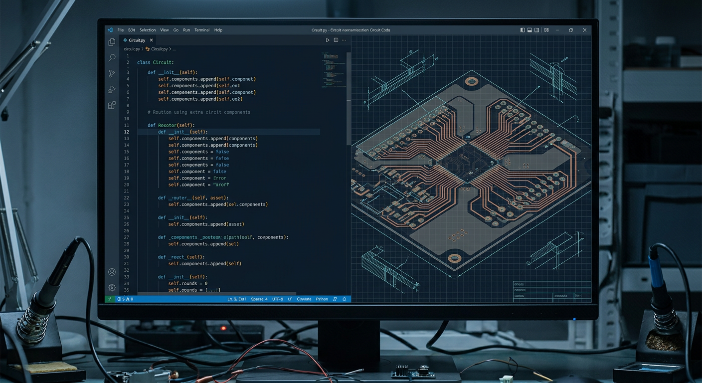
Recent traction around tools like Copperhead and Atopile across engineering forums has reignited a debate between GUI-based schematics and code-first hardware design. Software engineers building their first embedded devices look at traditional schematic capture tools like Altium, KiCad, or OrCAD and see an archaic, click-heavy relic from the 1980s. They want text files, version control diffs in Git, parametric subcircuits, and Cursor-style auto-completion for electronic components.
At the same time, experienced board layout engineers look at code-defined hardware with skepticism. A circuit board is not an abstract logical graph. It is a physical, three-dimensional electrodynamic system governed by Maxwell's equations, thermal dissipation, mechanical clearances, and manufacturing tolerances. When you describe a circuit entirely in text, you gain software modularity, but you risk disconnecting electrical intent from physical layout reality.
For a solo hardware engineer or a technical founder inside an early-stage startup, choosing how to capture and route your next board directly dictates your prototype schedule, respin budget, and manufacturing risk. Evaluating code-first electronic design automation requires separating real workflow gains from the persistent physics problems that code alone cannot solve.
The Promise of Code-Defined Electronics
Traditional schematic capture relies on visual diagrams. You place graphical symbols on a sheet, draw net wires between pins, assign footprints, and export a netlist to a PCB layout editor. This workflow works well for visual inspection, but it breaks down when managing complex variants, modular sub-circuits, and version control.
In standard EDA tools, visual schematics are stored in bloated XML, JSON, or proprietary binary formats. Running a git diff on a KiCad or Altium schematic file after moving three decoupling capacitors often produces hundreds of lines of coordinate noise. Branching and merging schematics across a team frequently results in unresolvable merge conflicts. Engineers end up locking design files or passing around monolithic revisions like main_board_v2_final_revB.kicad_sch.
Code-first tools like Atopile flip this model by defining electronic hardware as structured, object-oriented code. A microcontroller is not a square graphic on a canvas. It is a class with defined power rails, ground pins, and peripheral buses. A voltage regulator is a reusable module where input voltage, output voltage, and ripple targets are defined parametrically.
Consider an adjustable buck converter such as a Texas Instruments TPS62130. In a traditional GUI, an engineer places the IC, looks up the feedback equation in the datasheet, opens a calculator to select standard 1 percent E96 resistor values, manually updates the schematic values, and draws net wires to ground and output rails.
In a code-first DSL (domain-specific language), the engineer instantiates a buck module and declares the target output as 3.3V +/- 2%. The compiler runs the feedback equation, matches the output against standard component libraries, selects the optimal resistor divider, and validates that the inductor saturation current exceeds the peak switch current. If the system rail changes from 3.3V to 3.0V later in the project, updating a single line of text recalculates the passives across every downstream module.
This programmatic approach brings three real advantages to hardware teams:
- True Hierarchical Reuse: You can package a proven STM32 microcontroller subsystem with its crystal oscillator, decoupling capacitors, and SWD programming header into a modular software package. Reusing it across five different sensor nodes requires importing the package and passing configuration parameters rather than copy-pasting visual schematic blocks.
- Clean Git Collaboration: Pull requests show exact electrical changes. If an engineer changes a pull-up resistor from 10k to 4.7k ohms, the Git diff shows a one-line modification rather than thousands of altered coordinate tags.
- Automated Continuous Integration (CI): A compiler can check design rules on every commit. The CI pipeline can verify that all IC supply pins are connected to valid voltage sources, check that total current draw does not exceed regulator ratings, and validate that differential pairs match without an engineer ever opening an interactive GUI.
For peripheral integration and digital plumbing, this code-driven workflow saves significant design time. However, schematic capture represents only a fraction of hardware engineering. The real bottleneck in bringing a board to production is navigating the boundary where logical netlists meet physical layout.
Where Code Schematics Hit the Physical Wall
Code abstracts away physical implementation. In software, abstraction is power. In hardware design, abstraction can be fatal. A circuit board functions because of its physical geometry: copper thickness, dielectric constant, trace width, via barrel aspect ratios, and component placement relative to ground planes.
When hardware founders attempt to build entire production boards using purely programmatic tools, they run into five distinct physical failure modes.
1. Pin-Swapping and Spatial Routing Topology
Microcontrollers and FPGAs feature flexible pin multiplexing. An engineer can assign an I2C bus, UART peripheral, or PWM channel to dozens of different physical pins.
In a visual GUI layout workflow, the engineer places the MCU on the board, looks at the ratsnest of logical connections running to peripheral ICs, and swaps pin assignments in real time to prevent trace crossings. Pin-swapping on a 64-pin QFN or a 256-ball BGA can reduce layer counts from six layers down to four, eliminating blind vias and cutting fabrication costs by 40 percent.
In a code-first workflow, pin assignments are fixed in text before layout begins. If the initial code binds I2C1 to pins 12 and 13 on the north side of the chip, but the sensor IC sits on the south side, the layout tool must route traces around the entire package or drop vias through internal signal layers. Correcting this requires switching between the layout editor, the code file, and the MCU datasheet to find an alternate multiplexed pin that untangles the ratsnest. Without bidirectional spatial awareness, programmatic pin allocation creates tangled board routing.
2. High-Speed Return Paths and Ground Plane Discontinuities
A code compiler sees a net named SPI_CLK as an ideal mathematical conductor connecting Pin A to Pin B. It does not understand that at a 50 MHz clock rate with a 1-nanosecond rise time, the signal current travels through the copper trace while the high-frequency return current travels directly underneath on the reference plane.
If code-driven placement tools or basic autorouters route that clock trace across a split in the ground plane, the return path must take a long loop around the slot. This loop creates significant parasitic inductance, generates electromagnetic interference (EMI), and distorts signal edge rates, causing intermittent communication dropouts. An abstract netlist DSL does not contain spatial awareness of copper pours, return path geometries, or layer stackup dielectric heights.
3. Footprint Variations and Thermal Realities
Code abstractions often rely on idealized component definitions. A line of code declaring a 10uF 0402 ceramic capacitor ignores the non-linear realities of ceramic dielectrics. Under a 3.3V DC bias, a standard 6.3V-rated X5R 0402 capacitor can lose up to 60 percent of its effective capacitance. If your buck converter requires a true 10uF minimum capacitance for loop stability, that abstract code definition can lead to an unstable supply rail that oscillates under load.
Furthermore, high-current switching regulators require tight physical placement. The high di/dt loop consisting of the input bypass capacitor, high-side MOSFET, and low-side diode must have minimal loop area to prevent excessive voltage ringing and EMI. A compiler generating an abstract netlist does not enforce that the input capacitor must sit within 1 millimeter of the IC power pin on the top layer without intervening vias. When layout is decoupled from electrical capture, critical physical constraints get lost in translation.
4. RF Matching and Controlled Impedance Geometries
For boards containing Wi-Fi, Bluetooth, or Sub-GHz radios (such as an ESP32 or Semtech SX1262), the RF front-end demands precise transmission line geometry. You cannot define an RF trace as a simple point-to-point net.
The trace must be calculated as a coplanar waveguide or microstrip with controlled 50-ohm impedance, specific ground clearance rules, and continuous stitching vias along its perimeter. A software compiler generating board nets cannot guarantee impedance matching unless it directly reads the specific fab house stackup, prepreg dielectric constant (Er), and copper foil roughness.
5. Manufacturing Handoff and Contract Manufacturer Friction
When you send a design to an offshore PCB assembly house or an onshore quick-turn prototype plant, their CAM engineers do not review Python scripts or DSL definitions. They review standard Gerbers, ODB++ packages, pick-and-place centroid files, and traditional PDF schematics.
When code-first tools auto-generate visual schematics for human review, the output is frequently an unreadable, computer-generated spiderweb of nets. A manufacturing technician troubleshooting a dead board on a test bench relies on human-readable schematics with clear functional blocks, signal flow from left to right, and labeled test points. If your schematic looks like a machine-compiled net graph, fab house design-for-manufacturing (DFM) reviews take longer, and troubleshooting faulty prototypes burns valuable engineering hours.
Measuring Workflow Trade-Offs: GUI vs Code-First
To evaluate where programmatic hardware capture delivers real leverage and where it introduces friction, consider this illustrative composite of a typical 4-layer IoT sensor gateway design (microcontroller, cellular modem, power management, battery charging, and I2C sensor array).
| Design Phase | Traditional GUI EDA (Altium / KiCad) | Code-First EDA (Atopile / DSL) | Key Bottleneck / Failure Mode |
|---|---|---|---|
| Schematic Capture | 12 - 16 hours (manual symbol placement and wiring) | 4 - 6 hours (reusable modules and parametric passives) | Code capture is 2-3x faster for standard digital and power plumbing. |
| Component Selection & Validation | 6 - 8 hours (manual datasheet and stock lookups) | 2 - 3 hours (algorithmic passive calculation and constraints) | DSL tools catch component value errors early during compilation. |
| Design Rule Checking & CI | Manual ERC review at export; visual inspection | Automated CI pipeline on Git push; instant net checks | Code-first eliminates disconnected net errors and unpowered pins. |
| Component Placement & Pin Assignment | 6 - 8 hours (interactive visual pin-swapping and layout) | 12 - 16 hours (iterative text-to-layout pin-mux coordination) | Code lacks visual spatial feedback; pin-swapping across packages is tedious. |
| High-Speed & RF Routing | 8 - 12 hours (manual tuned traces, coplanar grounds) | 12 - 18 hours (manual intervention required; autorouters struggle) | Code cannot guarantee RF return paths or reference plane integrity. |
| DFM Audit & Fab Review | 2 - 4 hours (standard visual review and CAM export) | 4 - 6 hours (translating compiled schematics for CM technicians) | Contract manufacturers struggle to interpret auto-drawn schematics. |
| Total Time to Fab Handoff | 34 - 48 hours | 34 - 49 hours | Net time is comparable, but risk shifts from schematic bugs to layout errors. |
Note: The figures above represent an illustrative composite based on standard engineering turnaround times for mid-complexity 4-layer connected hardware prototypes.
The data reveals an important truth: code-first tools dramatically accelerate early schematic capture and component selection, but the time saved during capture is often eaten up during physical placement, pin optimization, and RF routing. The overall prototype timeline remains similar, but the failure modes shift from schematic logic bugs to physical layout and DFM defects.
A Decision Framework: When to Code and When to Click
Choosing the right capture method depends entirely on the electrical complexity, high-speed requirements, and physical constraints of your hardware.
                         ┌─────────────────────────────┐
                         │ Is your board primarily     │
                         │ standard digital buses and  │
                         │ low-speed modular I/O?      │
                         └──────────────┬──────────────┘
                                        │
                       ┌────────────────┴────────────────┐
                      YES                                NO
                       │                                 │
         ┌─────────────┴─────────────┐     ┌─────────────┴─────────────┐
         │ Does the design require   │     │ High-speed differential,  │
         │ extensive MCU pin-muxing  │     │ RF transceivers, or tight │
         │ or tight 3D enclosures?   │     │ power loop thermal layout │
         └─────────────┬─────────────┘     └─────────────┬─────────────┘
                       │                                 │
            ┌──────────┴──────────┐                      ▼
           NO                    YES            ┌───────────────────┐
            │                     │             │ Traditional GUI   │
            ▼                     ▼             │ Capture & Layout  │
  ┌───────────────────┐ ┌───────────────────┐   │ (Physics-First)   │
  │ Code-First DSL    │ │ Hybrid Approach   │   └───────────────────┘
  │ (Atopile / Code)  │ │ (Code logic with  │
  │ Fast Modular Dev  │ │ manual GUI layout)│
  └───────────────────┘ └───────────────────┘
Use this four-point checklist to decide whether a programmatic, code-first workflow fits your specific project:
- Board Architecture and Signal Speeds: If your design is an automated test fixture, an LED matrix driver, or an industrial sensor gateway with I2C, SPI, and RS-485 interfaces operating below 25 MHz, code-first capture delivers massive speedups. If your board features USB 3.0, PCIe, DDR4 memory, or multi-gigahertz RF paths, stay in a GUI-driven layout environment where physical trace geometry and continuous reference planes remain visible at all times.
- Density and Mechanical Enclosure Limits: If your PCB is loosely packed and fits into an off-the-shelf DIN-rail or standard enclosure, autorouting compiled code netlists will work cleanly. If you are packing a wearable device into a custom injection-molded enclosure with tight keepouts, odd board outlines, and dense QFN packages, manual placement and visual pin-swapping are mandatory.
- Component Reusability: If your company builds product families sharing 80 percent of their core architecture (such as an identical MCU core with varying sensor payloads), writing that core architecture in code creates a highly maintainable internal hardware library.
- Team Composition and Review Culture: If your hardware team consists of firmware engineers and full-stack developers building prototypes, code-first EDA fits cleanly into your GitHub pull-request workflow. If your team works with dedicated PCB layout specialists and external assembly houses, standard visual schematics prevent costly communication breakdowns.
What this means for IntelCAD
The split between code-first logic and visual physical layout highlights a fundamental reality: designing a circuit board requires both algorithmic abstraction and deep physical intelligence. Tooling should never force an engineer to choose between clean software version control and physical manufacturing readiness.
IntelCAD (intelcad.ai) bridges this gap by integrating physics-aware schematic capture, real-time bill-of-materials sourcing from distributors like DigiKey and Mouser, and automated layout that respects signal integrity, thermal dissipation, and fab house design rules. Rather than treating a circuit as raw code or flat pixels, layout automation must understand return paths, layer stackups, and component supply realities from the first net connection to the final Gerber export.
What to Watch Next
If you want to integrate code-driven workflows into your hardware development without compromising board reliability, monitor these developments over the coming quarters:
- Bidirectional Pin-Muxing Sync: Watch for code-first tools that introduce live back-annotation from layout tools. When you swap two pins in your PCB layout to untangle traces, the compiler should automatically update your schematic code and firmware pin-definition headers simultaneously.
- Constraint-Driven Code Compilers: Look for DSL compilers adding physical layout constraints directly into code syntax (such as declaring trace width, maximum loop inductance, and ground pour clearances within the component class).
- Automated DFM Linters for Code: Evaluate CI tools that can parse code-defined hardware and validate it against live tier-one PCB fab capabilities (such as JLCPCB, PCBWay, or Advanced Circuits design rules) before generating manufacturing outputs.
Code-first hardware design is transforming how engineers conceptualize and reuse electronic circuits. By understanding where text abstractions accelerate development and where physical layout demands direct spatial control, solo engineers can eliminate prototype respins and build robust production hardware faster.
Sources
- [1] Show HN: Copperhead, Cursor for circuit boards | Hacker News, https://news.ycombinator.com/item?id=49610059
- [2] Show HN: Atopile, Design circuit boards with code | Hacker News, https://news.ycombinator.com/item?id=39263854
- [3] Can AI design circuit boards yet? - Hacker News, https://news.ycombinator.com/item?id=49569366
- [4] Atopile Documentation and Architecture, https://atopile.io/
- [5] Atopile GitHub Repository, https://github.com/atopile/atopile
- [6] Code-Based PCB Design with AI: Inside atopile, https://www.youtube.com/watch?v=J1Dl5bUvm6E
- [7] Atopile Layout Integration Updates, https://atopile.io/blog/atopile-0-16-15