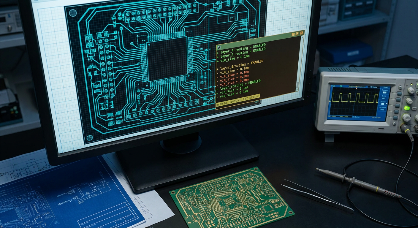
Run npm i -g copperhead, export an API key for Claude or OpenAI, open a git repository containing a KiCad project, and type copperhead do "add reverse-polarity protection on VIN".
Within twenty seconds, the tool inspects the root .kicad_sch file, identifies the DC input barrel jack, selects a P-channel MOSFET along with a zener diode and a pull-up resistor, writes the S-expressions directly into the schematic file, and runs an automated ERC check.
It feels identical to the first time you watched Cursor write a React component or refactor a Python class. Because KiCad 6, 7, 8, and the upcoming 9 releases use clean, plain-text S-expression syntax (.kicad_sch and .kicad_pcb), EDA files are suddenly accessible to large language models in the same way source code has been for the past three years.
The central question for anyone shipping physical hardware is simple: does natural language layout and schematic manipulation save an afternoon of tedious CAD work, or does it introduce silent, catastrophic errors that only reveal themselves when a board arrives from the assembly house with a dead microcontroller and a two-week respin penalty?
To answer that, you have to look at how these tools actually manipulate hardware description files, where plain-text LLMs break down on spatial physics, and how a working engineer can integrate agentic tools without blowing up a prototype run.
Why KiCad S-Expressions Are the New AST
For decades, commercial EDA suites treated their design files as opaque binaries or proprietary database formats. If you wanted to automate Altium Designer, you wrote Delphi scripts or Python automation against an unstable COM API. If you wanted to automate Cadence Allegro, you wrestled with SKILL scripts.
When KiCad overhauled its file architecture in version 6, it standardized everything on human-readable S-expressions. A resistor placed on a schematic is not an opaque byte stream. It is a text block:
(symbol
  (lib_id "Device:R_Small")
  (at 127.0 63.5 0)
  (unit 1)
  (exclude_from_sim no)
  (in_bom yes)
  (on_board yes)
  (dnp no)
  (uuid "8a3b2c1d-4e5f-6a7b-8c9d-0e1f2a3b4c5d")
  (property "Reference" "R4" (at 129.54 62.23 0)
    (effects (font (size 1.27 1.27)) (justify left))
  )
  (property "Value" "10k" (at 129.54 64.77 0)
    (effects (font (size 1.27 1.27)) (justify left))
  )
  (property "Footprint" "Resistor_SMD:R_0402_1005Metric" (at 127.0 63.5 0)
    (effects (font (size 1.27 1.27)) hide)
  )
  (pin "1" (uuid "1b2c3d4e-5f6a-7b8c-9d0e-1f2a3b4c5d6e"))
  (pin "2" (uuid "2c3d4e5f-6a7b-8c9d-0e1f-2a3b4c5d6e7f"))
)
To a language model trained on millions of GitHub repositories, this syntax looks like Lisp. The model understands tokens, nested parentheses, coordinate transforms, and key-value attributes.
Copperhead exploits this direct access. Instead of compiling an intermediate language down to KiCad, as code-to-PCB frameworks like Atopile do, it treats your existing schematic and layout files as mutable codebases. It reads the files into context, generates unified diffs against the S-expressions, writes the modified files to disk, and then shells out to kicad-cli to run Electrical Rules Checks (ERC) and Design Rules Checks (DRC).
If the rule check passes without errors, the agent presents you with a git diff. You review the schematic visually in KiCad, accept or reject the commit, and move on.
On simple, deterministic modifications, this workflow is fast. If you prompt it to add 5.1k pulldown resistors to the CC1 and CC2 pins of a USB Type-C receptacle, it finds the receptacle symbol, checks the pin assignments, instantiates two 0402 resistors, wires pin 1 of each to CC1 and CC2, ties pin 2 of both to ground, and assigns standard LCSC part numbers. It avoids five minutes of manual component searching, wire routing, and footprint assignment.
Hardware design, however, is not software engineering. In software, if a function compiles, satisfies type constraints, and passes unit tests, it usually runs. In PCB design, a schematic can be electrically complete, pass every ERC check with zero warnings, and still produce a completely non-functional board.
The Four Failure Modes of LLM Circuit Edits
When an LLM edits a codebase, a logic error triggers an exception or a failing integration test. In hardware, an LLM error often produces a silent layout bug that bypasses DRC entirely.
Over several test runs modifying a four-layer ESP32-S3 and TI MSPM0 mixed-signal board, four specific failure patterns emerged repeatedly.
1. Hierarchical UUID Mismatches and Ghost Nets
KiCad 8 relies heavily on Universally Unique Identifiers (UUIDs) to map pins on a schematic sheet to physical footprints and nets on the layout canvas. When you copy and paste a subcircuit in the GUI, KiCad regenerates these UUIDs behind the scenes to prevent collisions.
When an LLM edits a .kicad_sch file directly, it must generate new valid UUIDs for every newly instantiated symbol, wire, label, and pin. If the model accidentally duplicates a UUID from another sheet or reuses an existing net identifier on a different physical net, KiCad can silently merge two separate nets without generating an explicit visual warning.
In one test case where Copperhead was asked to duplicate an analog front-end channel (an op-amp gain stage with four passive components), the model duplicated the schematic block and updated the reference designators from R12 to R18. However, it left the internal pin UUIDs of the feedback loop identical to channel 1.
When the netlist was updated in the layout editor via kicad-cli --netlist, the ratsnest showed channel 2's inverting input shorted directly to channel 1's feedback node across the board. The ERC script did not flag it because both nets were formally tied to valid output drivers, meaning the schematic appeared electrically consistent to the checker.
2. The Microcontroller Pin Swap Trap
One of the most common layout tasks is swapping GPIO pins on an MCU to untangle a ratsnest and avoid layer transitions. A prompt like "Swap the SPI and UART pins on U1 to eliminate the trace crossings going to header J3" seems like the ideal agentic task.
An LLM will parse the symbol, read the pin names, swap the net connections between GPIO4/GPIO5 and GPIO18/GPIO19, and update the schematic labels cleanly.
[Prompt: Swap SPI1_MOSI and UART0_TX to clean up routing]

Before:
  MCU Pin 12 (GPIO4, ADC1_CH3, SPI1_MOSI) -> SPI Bus
  MCU Pin 25 (GPIO18, UART0_TX)           -> Debug Header

After LLM Edit:
  MCU Pin 12 (GPIO4, ADC1_CH3, SPI1_MOSI) -> Debug Header
  MCU Pin 25 (GPIO18, UART0_TX)           -> SPI Bus
Electrically, this passes ERC without issue. But the LLM often lacks awareness of underlying silicon constraints:
- Hardware Boot Strapping: Swapping a general UART pin to a pin like
GPIO0orGPIO2on an ESP32 can pull a strapping pin high or low during power-up, locking the microcontroller in a permanent bootloader reset loop. - Alternate Function Multiplexing: On modern microcontrollers like the STM32G4 or TI MSPM0, not every pin can map to hardware SPI DMA channels. If the model moves a hardware SPI bus to a GPIO that only supports software bit-banging, the firmware team loses hardware DMA support.
- ADC Input Attenuation: Moving an analog sensor trace to an open GPIO pin might land it on a pin that lacks internal ADC routing or shares an ADC channel with an internal temperature sensor.
Unless your prompt includes the entire 150-page pinout matrix and multiplexing chapter of the MCU datasheet in its context window, an agentic tool will treat all GPIO pins as fungible digital lines. They are not.
3. Decoupling Loop Inductance and High-Frequency Return Paths
Language models operate on abstract graphs. They understand that pin 1 of capacitor C5 must connect to VDD33 and pin 2 must connect to GND.
They have no innate understanding of Maxwell's equations, parasitic inductance, or return current loop areas.
When prompted to add decoupling capacitors to a switching regulator or an MCU, an agent will place the components on the board wherever there is open coordinate space that satisfies bounding-box DRC clearances. In our testing, the agent placed a 100nF high-frequency bypass capacitor 12mm away from the MCU power pin, routing the power trace through two vias and across an unbroken slot in the internal ground plane.
From a DRC perspective, the trace had 0.15mm clearance, the annular rings were within fab limits, and the nets were connected. From an RF and signal integrity perspective, that 12mm loop added roughly 8nH of parasitic trace inductance, rendering the decoupling capacitor useless at 100MHz clock harmonics and creating an unintentional EMI radiator.
Bad Agent Placement:
[Power Pin] ---- 12mm trace ---- (Via to L2) ---- (Via to L1) ---- [0402 Cap] ---- (Via to GND)
Parasitic Inductance: ~8nH to 10nH (Bypass capacitor fails above 30MHz)

Correct Layout:
[Power Pin] == 0.8mm trace == [0402 Cap] == (Via directly to solid L2 Ground Plane)
Parasitic Inductance: < 0.8nH
Automated routing tools and LLM layout scripts can check for geometric overlap, but they do not calculate dynamic loop inductance unless paired with an integrated electromagnetic field solver.
4. Thermal Relief and Pad Apertures
Another failure point is footprint and thermal relief generation. An agent modifying a .kicad_pcb file can easily place ground vias into an exposed thermal pad (such as the EPAD on a QFN-32 package).
If the agent fails to specify soldermask tenting on the bottom side or does not coordinate via drill size with standard fab plugging rules (e.g., specifying a 0.3mm hole without solder mask plugging), solder paste will wick down the via barrels during reflow. This starves the component of solder, resulting in poor thermal dissipation and intermittent ground connections under the IC.
Standard DRC engines in KiCad do not flag open via barrels in thermal pads as errors. They see copper touching copper. It is a pure manufacturing and assembly constraint that requires human verification or strict DFM rule decks from the assembly house.
Code-to-PCB vs. Direct S-Expression Mutation
Copperhead represents one side of an ongoing architectural split in AI-assisted electronic design.
| Approach | Mechanism | Representative Tools | Strengths | Weaknesses |
|---|---|---|---|---|
| Direct S-Expression Mutation | LLM acts on raw .kicad_sch and .kicad_pcb files via text diffs. |
Copperhead | Zero lock-in. Works directly on existing git repositories and standard KiCad files. | High risk of hallucinated syntax, UUID breaks, and spatial layout blind spots. |
| Code-to-PCB Compilers | Engineer writes in a DSL (Python/Atopile/JITX) which compiles to netlists and footprints. | Atopile, JITX | Strict type safety, modular software patterns, parametric component reuse. | Steep learning curve; completely replaces standard GUI schematic workflows. |
| Geometric Routing Engines | Dedicated solvers and rule-based algorithms handle routing and placement natively. | IntelCAD, DeepRoute | Deterministic signal integrity, high-speed differential pair matching, zero LLM syntax drift. | Focuses on layout/routing execution rather than conversational schematic ideation. |
Frameworks like Atopile take a programmatic stance: you write code, define pin-to-pin assertions, and compile down to a board. The advantage is strict type checking. If you connect a 3.3V GPIO to a 5V rail without a level shifter, the compiler halts before generating a PCB.
Copperhead takes the pragmatic route: keep the visual KiCad workflow that millions of engineers already know, but add an interactive terminal copilot that speeds up manual file changes.
For a solo engineer running a hardware startup, direct S-expression mutation is immediately usable because it does not require rewriting legacy component libraries into a domain-specific programming language. But that convenience demands a rigorous verification protocol before sending files to a board house.
How to Safely Integrate an EDA Copilot into Your Workflow
If you want to use an LLM agent like Copperhead on production boards, you cannot treat it like an auto-pilot. You must treat it like an over-confident junior intern who knows S-expression syntax perfectly but has never held a soldering iron or looked at a thermal camera.
Here is a practical workflow that captures the speed gains while guarding against respin risks.
1. Constrain the Agent to Modular Subcircuits
Do not ask an agent to "design the power supply section." That prompt is an invitation for missing thermal dissipation calculations, incorrect inductor saturation current ratings, and bad feedback trace routing.
Instead, use the agent for well-defined, repetitive tasks where the input and output constraints are explicit:
- "Add an ESD protection diode array (USBLC6-2SC6) across the USB D+, D-, and VBUS lines with decoupling close to connector J1."
- "Instantiate four 10k 0402 pull-up resistors on the I2C bus lines connected to 3V3_AUX."
- "Create a standard 6-pin 1.27mm SWD programming header connected to the SWDIO, SWCLK, NRST, and GND pins of U2."
These bounded prompts have clear net boundaries and little spatial ambiguity.
2. Isolate Every Change in a Dedicated Git Branch
Never run an agentic EDA tool on your main development branch. Before running copperhead do, ensure your git working tree is clean:
git checkout -b copilot-add-tvs-protection
copperhead do "add USBLC6-2SC6 to USB data lines"
Use visual diffing tools rather than standard text diffs to review the results. While git diff shows you the raw S-expression changes, running kicad-cli to export SVG or PDF renders of the modified schematic sheets allows you to run a side-by-side visual comparison with git-diff-image or PlotKicadSch.
# Verify schematic consistency via headless CLI
kicad-cli sch erc --severity-all --exit-code-violations project.kicad_sch
If the headless ERC fails, discard the commit immediately. Do not spend twenty minutes debugging an LLM's broken UUID tree; rollback and write the change manually or refine the prompt.
3. Maintain Hard Physical Routing Boundaries
Let the agent handle schematic edits, BOM metadata generation, and footprint assignments, but maintain strict human ownership over critical board layout tasks:
- High-Speed Differential Pairs: USB 2.0 (90-ohm differential), USB 3.0 / PCIe (85-ohm differential), and Ethernet traces require strict phase matching, length tuning, and controlled impedance stackups. An LLM cannot accurately calculate the microstrip differential impedance without a precise stackup definition (such as a standard JLCPCB JLC04161H-7628 4-layer stackup) and field solver equations.
- Switching Power Topologies: The high di/dt loop of a synchronous buck converter (input capacitor -> high-side FET -> low-side FET -> ground return) must be routed on a single top layer with wide copper pours and minimal via count. Do not allow an agent to autoroute these nodes.
- Sensitive Analog Nodes: Keep op-amp summing junctions, voltage divider feedback nodes, and crystal oscillator load capacitors entirely in human hands.
+-------------------------------------------------------------+
|                  SAFE FOR AGENTIC AUTOMATION                |
|  - BOM metadata & LCSC part numbering                       |
|  - Pull-up / pull-down resistor arrays                      |
|  - ESD diode instantiation & connector mapping              |
|  - Power LED & indicator subcircuits                        |
|  - Mechanical mounting hole placement                       |
+-------------------------------------------------------------+
|                 REQUIRES MANUAL ENGINEERING                 |
|  - Switching regulator switch-node loops & inductor routing |
|  - High-speed differential pair impedance & length matching |
|  - MCU bootstrapping & alternate function pin allocations   |
|  - RF antenna matching networks & 50-ohm coplanar guides    |
|  - Thermal via arrays & paste mask aperture sizing          |
+-------------------------------------------------------------+
The Real Economics of Board Respins
When a software deployment fails, you rollback the commit, patch the bug, and redeploy in ten minutes. The cost is negligible.
When a four-layer PCB fails because an agent swapped an I2C pin to an input-only GPIO or routed a crystal load trace through an internal ground plane split, the economics look very different:
- Fabrication and Assembly: $150 to $400 for a fast-turn 5-board prototype run at an assembly house (including setup fees, SMT stencils, and DHL shipping).
- Component Write-offs: $50 to $200 in lost silicon, especially if an expensive MCU or FPGA cannot be easily desoldered from a damaged board.
- Engineering Time: 15 to 25 hours spent probing test points with an oscilloscope, cutting traces with a scalpel, running blue-wire rework under a microscope, and tracking down the root cause.
- Schedule Slip: 8 to 14 business days waiting for the revised fab run to clear assembly and customs.
A single silent netlist bug easily costs $1,500 in direct labor and delays customer milestones by two to three weeks.
Tools like Copperhead represent an important step forward for hardware engineering. The ability to query, modify, and document a complex KiCad project directly from a terminal or CI/CD pipeline removes hours of low-level data entry. But until language models incorporate spatial physics, electromagnetic boundary conditions, and deep silicon-level pin multiplexing constraints directly into their reasoning loops, the engineer holding the schematic review checklist remains the only line of defense against an expensive box of scrap copper.