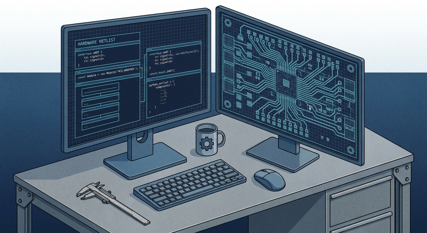
The launch of Copperhead on Hacker News as an AI code editor for circuit boards has reignited a debate among solo hardware engineers. The pitch is familiar to software developers: replace the graphical point-and-click schematic canvas with a TypeScript or Python development environment that handles circuit generation, component reuse, and git version control like standard software.
For an electrical engineer operating as the sole hardware builder inside a startup, the appeal is obvious. Visual schematic capture in legacy tools has always struggled with clean version control. A single moved resistor in Altium or KiCad can alter hundreds of lines of XML or S-expression files, making pull request diffs nearly useless. Parametric sub-circuits, such as multichannel sensor inputs or repetitive power regulation stages, often require tedious manual copy-pasting.
Text-based electronic design automation promises to solve these workflow headaches. By treating schematics as software objects, tools like Copperhead, JITX, and atopile let engineers instantiate circuit blocks through functional code. Yet the transition from code-defined netlists to physical copper on FR4 exposes severe ergonomic limits. Circuit boards are not abstract logical graphs. They are physical, electromagnetic, and thermal objects where geometry dictates electrical behaviour.
Deciding whether to adopt a code-first EDA tool comes down to understanding where programmatic capture accelerates development and where it introduces fatal blind spots before the layout stage.
Where Code-First Schematics Win
Text-based capture excels in areas where electronics mimic pure software logic: hierarchical repetition, mathematical sizing, and configuration management.
Consider an industrial telemetry board requiring eight identical isolated 4-20mA sensor interfaces. In traditional visual capture, an engineer places eight identical operational amplifier blocks, assigns net names, updates reference designators, and manually verifies that component values match across every channel. When a filter capacitor value changes from 100nF to 10nF after lab testing, the engineer must update eight individual sheets or risk an assembly mismatch.
// Programmatic generation of an 8-channel analog input block
import { OperationalAmplifier, Resistor, Capacitor, Net } from "copperhead-eda";

export function AnalogInputStage(channelCount: number, cutoffFreqHz: number) {
  const stages = [];
  for (let i = 0; i < channelCount; i++) {
    const r1 = new Resistor({ resistance: "10k", tolerance: "1%", package: "0402" });
    const c1 = new Capacitor({ capacitance: `${1 / (2 * Math.PI * 10000 * cutoffFreqHz)}F`, package: "0402" });
    const opamp = new OperationalAmplifier({ partNumber: "OPA320AIDBVR", package: "SOT-23-5" });

    // Establish net connections
    Net.connect(r1.pin2, c1.pin1, opamp.nonInvertingInput);
    stages.push({ r1, c1, opamp });
  }
  return stages;
}
In code, this entire subsystem is a parameterized function. Changing the filter cutoff frequency takes one parameter edit. The compiler calculates component values, checks power dissipation against resistor ratings, and instantiates the components without manual mouse clicks.
Version control becomes clean. Git commits show readable diffs of code logic rather than binary blobs or massive coordinate dumps. Code reviews happen in standard pull requests where peer engineers can verify net connections, component ratings, and logic flow line by line.
For digital interfaces, pin mapping validation also gains speed. When wiring a 100-pin microcontroller to peripheral buses, a programmatic script can iterate through GPIO assignments and check pin multiplexing against alternate peripheral tables instantly, preventing the classic mistake of assigning two high-speed SPI buses to overlapping hardware pins.
The Physical Disconnect in Text-Driven Capture
The advantage of code-first design breaks down as soon as net connectivity intersects with board physics. A visual schematic is not just a connectivity list. It is a spatial document that communicates electrical intent to the layout engineer.
When looking at a well-drawn visual schematic of a buck converter, the spatial layout immediately signals critical current loops. The input bypass capacitor sits directly adjacent to the high-side MOSFET drain and the low-side switch source. The feedback voltage divider is drawn far away from the noisy inductor switching node, indicating that the feedback trace must avoid the high dv/dt plane on the board.
In pure text, that spatial intent disappears into a list of node connections:
// Logical connection loses the critical spatial relationship
Net.connect(buckController.VFB, rTop.pin2, rBottom.pin1);
Net.connect(buckController.SW, inductor.pin1, snubberCap.pin1);
To a text compiler, a connection between three pins is an ideal node with zero resistance, zero parasitic inductance, and zero coupling capacitance. To a physical board running at 2 MHz switching speeds, the loop area between the input capacitor, the switching pin, and ground determines whether the product passes CISPR 32 Class B electromagnetic compliance or radiates broad-spectrum noise that fails regulatory testing.
When the netlist is compiled from code and passed to a layout environment, the routing tool or the human layout engineer receives only a flat netlist. Without embedded spatial placement hints or visual hierarchy, the layout engineer must reconstruct the physical intent from component datasheets, defeating the time saved during schematic capture.
The Feedback Loop Penalty
The separation between code generation and physical layout creates severe feedback penalties during routing. High-density designs with tight microcontrollers or field-programmable gate arrays often require iterative pin swapping to untangle traces on inner routing layers.
| Design Task | Visual Schematic Workflow | Text-Based Code Workflow |
|---|---|---|
| Pin Swapping | Click two pins on MCU symbol, swap nets, push updates to PCB layout in 5 seconds. | Edit code net assignments, recompile project, re-import netlist, re-verify routing paths. |
| Bypass Placement | Place decoupling cap visually beside power pin on sheet; layout tool groups components. | Tag capacitor object with metadata rules; rely on layout engine to interpret clustering constraints. |
| Differential Pair Routing | Draw differential wire pair, label _P and _N, visual tool applies 100-ohm rule immediately. |
Define differential net object in code, assign routing class parameters, check post-route impedance. |
| DFM Clearance Checking | Real-time DRC overlays visual warnings directly on pads and copper pours. | Compiler flags clearance violations during text build, requiring context switch back to layout editor. |
In visual tools, an engineer routing a 48-pin QFN can swap adjacent GPIO pins while viewing the unrouted ratlines directly on the PCB. The graphical schematic and the board layout stay synchronized through bi-directional cross-probing. In a code-first pipeline, swapping two pins requires context-switching back to the source code, locating the assignment variables, recompiling the netlist, and refreshing the layout canvas. This friction compounds across dozens of routing channels.
High-Speed Routing and Impedance Geometry
High-speed signals expose the largest ergonomic gap in text-first workflows. Modern microcontroller and processor designs regularly route USB 2.0 High Speed (480 Mbps), PCIe Gen 2/3, and DDR4 memory buses. At these speeds, traces are transmission lines, not abstract connections.
Designing a USB differential pair requires matching trace lengths within 0.15 mm, maintaining a continuous reference plane across layer transitions, and preventing impedance discontinuities caused by reference plane splits.
While a code-first environment can define routing constraints programmatically (such as specifying a 90-ohm differential target and maximum skew limits), it cannot foresee the mechanical obstacles on the physical board. When a differential pair encounters a structural mounting hole or a dense connector pinfield, the routing path must divert.
In visual layout, the engineer observes the detour immediately, places ground return vias next to the signal vias, and applies serpentine delay tuning interactively while monitoring the real-time length-tuning bar. Doing this through text-based constraint files forces the engineer into an awkward split: writing rules in text, checking physical geometry in a viewer, and hand-adjusting routing in a graphical tool that may not feed spatial alterations back into the source code cleanly.
If the layout tool alters the routing topology to resolve an impedance mismatch, how is that physical change reflected back in the declarative TypeScript model? If the code remains the single source of truth, every manual layout adjustment risks being overwritten on the next compile cycle unless the tool implements robust bi-directional AST (Abstract Syntax Tree) synchronization.
Mechanical Enclosures and Thermal Floorplanning
Printed circuit boards are 3D mechanical components before they are electrical circuits. For solo hardware engineers designing products for compact industrial housings or consumer devices, the board outline, connector locations, and component height limits dictate the design.
Consider an IoT device fitting inside an IP67 waterproof enclosure:
- USB-C receptacle must sit flush against the silicone gasketed opening.
- Indicator LEDs must align with light pipes molded into the top enclosure shell.
- Large electrolytic capacitors and inductors must avoid structural ribbing inside the lid.
- Power amplifier modules must contact the aluminium base plate through thermal gap pads.
Visual capture allows the engineer to establish a spatial floorplan early. By looking at a schematic alongside a 3D board view, the engineer groups thermal sources and separates noisy digital switching from sensitive analog front-ends.
Code-first tools often treat component placement as a downstream constraint solver problem. While layout engines can solve basic packing problems, automated placement algorithms struggle with multi-domain physical trade-offs. An algorithm might place a switching inductor right next to an enclosure screw boss to minimize trace length, failing to account for the mechanical stress caused by fastener torque, or place a high-gain microphone preamp directly beneath a high-speed clock oscillator.
Handling these spatial constraints in text requires verbose, brittle coordinate declarations:
// Brittle spatial constraints in code
Component.setPlacement("J1", { x: 0, y: 25.4, side: "top", locked: true });
Component.setPlacement("LED1", { x: 12.5, y: 5.0, rotation: 90 });
Component.keepoutArea({ x1: 20, y1: 10, x2: 35, y2: 25, layers: ["top", "inner1"] });
Declaring absolute coordinates in text code defeats the productivity gains of code reuse. If the board outline changes by 2 mm to accommodate a thicker gasket, all hard-coded coordinate offsets break. Graphical EDA tools handle this organically through mechanical DXF/STEP imports, constraint managers, and interactive snap grids.
The Live Sourcing and BOM Availability Problem
Hardware development in real-world supply chains requires continuous part substitutions. A solo engineer cannot rely on static library definitions because component inventory fluctuates daily.
If an active 3.3V LDO regulator goes out of stock at distributors like Digi-Key or Mouser during schematic capture, the engineer must immediately identify an alternate part. That swap involves checking:
- Pin-for-pin compatibility.
- Dropout voltage under full load.
- Thermal pad ground requirements.
- Minimum output capacitance and ESR stability ranges.
Visual EDA environments increasingly integrate live distributor APIs directly into the component selector window. When picking a part, the engineer sees real-time pricing, stock levels across distributors, and active lifecycle status (Active, NRND, Obsolete).
In text-first EDA, third-party component libraries are defined in code packages or central repositories. If a part number in the code is obsolete or has an 18-week lead time, the compiler will not flag an issue unless the code tool maintains a live query pipeline to distributor APIs during the build step.
Furthermore, modifying a component package in code requires updating the underlying pinout mapping. If an engineer replaces a SOT-23 LDO with a DFN-6 package because the SOT-23 is out of stock, they must ensure the programmatic footprint declaration correctly maps pins (e.g., exposed thermal pad mapped to GND). In a visual tool, the pin-to-pad mapping matrix is graphically inspectable before passing to layout. In code, an indexing error in a pin array can short power to ground on fabrication day.
A Pragmatic Decision Matrix: When to Code, When to Draw
Code-first EDA tools are not an all-or-nothing proposition. They are powerful additions to an engineering toolkit when applied to the right problem domains.
                          Is your design primarily:
                                     │
        ┌────────────────────────────┴────────────────────────────┐
        ▼                                                         ▼
 Repetitive / Logical                               Physical / High-Density
 (e.g., LED matrices,                              (e.g., dense RF boards,
  multi-channel ADC,                                 power electronics, tight
  algorithmic pin mapping)                           mechanical enclosures)
        │                                                         │
        ▼                                                         ▼
 Use Code-First EDA                                 Use Visual Schematic Capture
  • Instant parameter scaling                        • Direct spatial awareness
  • Clean Git diffs and PRs                          • Interactive impedance control
  • Reusable functional blocks                       • Real-time DFM/clearance feedback
When Code-First Capture Outperforms:
- Modular, algorithmic circuits: LED video wall drivers, battery management system cell-balancing channels, and large test fixtures with repetitive pin banks.
- Highly parameterized sub-modules: Power supply stages where component values scale directly from input voltage formulas.
- Software-dominated teams: Multi-disciplinary teams where firmware and software engineers need to inspect hardware changes via GitHub or GitLab pull requests without installing heavy desktop CAD suites.
When Visual Schematic Capture Remains Superior:
- Mixed-signal and RF layouts: Systems where grounding topologies, star-point connections, and trace shielding require tight visual coordination.
- Space-constrained consumer hardware: Products where board outlines follow complex 3D housings, requiring frequent cross-probing between schematic nets and 3D enclosure clearances.
- High-speed digital buses: Designs incorporating high-speed interfaces with tight skew matching and impedance requirements.
- Fast prototype turnaround: Weekend prototypes where grabbing verified visual symbols and footprints from established community libraries is faster than writing or debugging code definitions.
What This Means for IntelCAD
The emergence of text-based tools like Copperhead demonstrates that engineers are hungry for automation, version control, and faster schematic authoring. But translating text into a working physical circuit board requires more than abstract syntax parsing.
IntelCAD bridges this gap by combining automated, physics-aware routing with real-world manufacturing constraints. Rather than forcing engineers to choose between brittle text coordinates and manual mouse-driven routing, the platform applies automated layout algorithms that understand return path physics, layer stackups, and live component availability from major distributors. The objective is not just generating a netlist quickly, but ensuring the resulting board passes DRC, handles high-speed impedance requirements, and can be manufactured on standard SMT lines without respin delays.
The Ergonomic Horizon
Text-based electronic design will not eliminate visual schematics overnight, nor should it. Graphical circuit diagrams serve as a universal language for electrical engineers, conveying physical, functional, and safety relationships that code netlists flatten.
The real breakthrough in design automation is not forcing hardware into a pure text editor. It is building bi-directional environments where an engineer can write code to generate repetitive blocks, instantly see the visual schematic topology, and interactively route traces with automated layout engines that respect copper physics.
Until code-first tools can seamlessly merge physical impedance, 3D mechanical clearance, and component supply realities into the compilation loop, solo engineers should use text capture where it shines on modular blocks, while keeping visual tools on hand to verify physical reality before ordering bare boards from the fab.
Common Questions
Can text-based EDA completely replace visual schematics for production hardware? No. While text-based tools accelerate modular block creation and parametric circuit sizing, they lack the spatial awareness required for complex high-speed return paths, thermal layouts, and tight 3D mechanical integration.
What is the main risk of using code-first EDA tools? The primary risk is the loss of physical intuition during capture. Programmatic netlists treat connections as zero-impedance logical nodes, which can lead to severe noise, EMI, and signal integrity failures if the layout stage is not carefully verified against real-world physics.
Sources
- Hacker News: Copperhead, Cursor for circuit boards: https://news.ycombinator.com/item?id=49610059
- pcbGPT: Automatic PCB Schematic Synthesis from Natural Language: https://arxiv.org/html/2606.01188v1
- Next-Gen Tools for Electronics Design: https://219design.com/6-next-gen-tools-for-electronics-design/
- Altium PCB Design Process and EDA Approach: https://resources.altium.com/p/pcb-design-process-the-eda-design-approach
- Proteus Schematic Capture and Design Capabilities: https://www.labcenter.com/schematic/