Over the past two weeks, updated benchmarks and comparison runs between Quilter, DeepPCB, and legacy speculative routers have circulated across hardware engineering forums. The headline metrics look impressive at first glance. Modern machine learning engines can ingest an unrouted netlist, place components, and hit 100 percent completion on a complex four-layer micro-controller board in under twenty minutes. For a solo hardware engineer buried under schematic capture, component sourcing, firmware bring-up, and mechanical enclosure clearances, that speed sounds like instant relief.
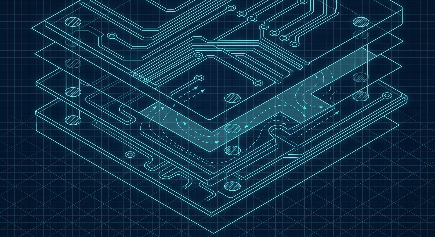
Yet when you export those completed layouts into a 2D field solver or inspect the Gerber files on an assembly review screen, the euphoria vanishes. The nets connect pin-to-pin without a single design rule check (DRC) clearance violation. But the internal ground planes resemble Swiss cheese. Return paths meander across layer boundaries without stitching vias. Copper pours around switching regulators are choked by narrow necks, and high-speed traces cross split planes with zero reference continuity.
For an engineering team operating on tight venture capital or a strict client deliverable, a board that connects logically but fails electrically is worse than an unrouted board. A manual layout delay costs three days of engineering time. A respin caused by radiated emissions failures, ground bounce, or localized thermal throttling on an unpoured power stage costs three weeks and thousands of dollars in prototype stencils, assembly setup fees, and expedited fab turns.
Understanding why reinforcement learning and neural routing models still stumble over ground returns and copper pours requires looking past the marketing demos and inspecting the core mathematical formulations behind these tools.
The Mathematical Disconnect: Graph Connectivity vs Electromagnetic Physics
Traditional autorouters, like the legacy Specctra or modern topological gridless engines, treat routing as a shortest-path search problem across a constrained geometric space. They use variants of Dijkstra, A-star, or Lee algorithms to find paths that do not collide with keepout zones or existing copper traces.
Modern AI-driven tools take two distinct technological paths, but both inherit a foundational blind spot.
DeepPCB relies primarily on deep reinforcement learning (RL) agents trained on grid-based board representations, treating PCB routing similarly to image-to-image translation and board-state search. The reward function rewards completing nets, penalizes DRC clearance violations, and penalizes total trace length and via count.
Quilter takes a physics-inspired approach combined with reinforcement learning and generative search. It places components and routes traces concurrently by spawning dozens of candidate solutions in parallel, evaluating thermal dissipation, basic parasitics, and DRC rules to converge on an optimized layout.
Both approaches represent massive engineering steps beyond 1990s maze routers. However, they struggle with high-frequency return paths and dynamic copper pours because their primary loss functions are topological rather than electromagnetic.
In digital logic, a net is a single mathematical node that connects pin A to pin B. In physical reality, a signal is an electromagnetic wave propagating through a transmission line formed by the trace and its immediate reference plane. The return current does not follow the path of lowest DC resistance. Above roughly 100 kHz, return current follows the path of lowest loop inductance, which sits directly beneath the signal trace on the adjacent reference copper.
When an AI routing agent evaluates a candidate trace route, its reward engine typically asks three simple questions:
- Does this trace violate minimum trace-to-trace or trace-to-pad clearances?
- Did this trace successfully reach the target pad?
- How much did this trace add to the total board trace length and via budget?
The agent does not calculate the dynamic high-frequency loop area of the return current in real time. Running a full 3D or quasi-static 2D Maxwell field solver at every step of a reinforcement learning search tree is computationally intractable. A single board route involves millions of exploratory branch decisions. If evaluating each step required an electromagnetic field solver run, routing a simple STM32 board would take three months of high-performance GPU cluster time instead of fifteen minutes.
To run quickly, AI engines use proxy heuristics. They assume that if an unbroken copper pour exists somewhere on layer 2, any trace routed on layer 1 automatically has an adequate reference. That assumption is mathematically cheap, and electrically dangerous.
Three Failure Modes in AI-Generated Planes and Returns
When AI engines place traces and generate copper planes without field-level physical awareness, layouts consistently degrade in three specific areas.
1. Return Path Fragmentation via Dense Via Clusters
AI routing agents treat vias as inexpensive mathematical escape hatches. When an agent encounters congestion on the top layer, it drops a via pair, hops to an internal signal layer or bottom layer, routes through an open channel, and drops back up.
While Quilter and DeepPCB try to penalize excessive via counts, their reward algorithms will always choose a via over an unrouted net. On dense microcontroller pin breakouts or near BGA packages, the engine frequently drops eight to twelve vias in a tight cluster.
Each via requires an antipad, which is the clearance void drilled through the internal copper plane to prevent the via barrel from shorting to the plane. When ten vias are placed 0.8 mm apart with 0.2 mm antipad clearances, their antipads merge into a single continuous slot in the ground plane.
If high-speed SPI, USB data, or PWM clock lines are routed across that slot on an adjacent layer, their high-frequency return currents cannot flow underneath them. The return current is forced to divert around the entire antipad slot, creating a large parasitic loop antenna. The result is instant radiated emissions failures during CISPR 32 testing and elevated ground bounce that can cause random digital resets on adjacent logic pins.
2. Copper Pour Starvation and Isolated Peninsulas
Manual PCB designers typically lay down continuous reference planes first, route critical high-speed and power nets with dedicated return paths, and then pour ground and power copper into remaining areas with careful attention to neck widths and thermal ties.
Many AI autorouting pipelines reverse or distort this workflow. They route all signal traces across available layers and flood the remaining empty spaces with polygon copper pours at the final generation step.
This creates copper starvation. The AI agent routes traces through the center of open channels, cutting the available ground copper into narrow peninsulas, slivers, and isolated islands. When copper floods through a 0.15 mm gap between three signal traces, that narrow neck introduces high DC resistance and parasitic inductance. If that neck is the only connection tying a decoupling capacitor's ground pad back to the main ground plane, the capacitor is effectively decoupled from the circuit. Its low-impedance path to ground is broken by the inductance of the copper sliver.
3. Asymmetric Ground Loops on Switching Regulators
Buck converters, boost regulators, and motor drive circuits require tight, low-inductance loop geometry. The high-di/dt loop formed by the input capacitor, high-side MOSFET, low-side switch, and ground return must be as physically compact as possible.
AI engines that optimize purely for net-to-net Euclidean distance frequently place the input decoupling capacitor three to five millimeters away from the switching regulator's VIN and PGND pins, routing them with standard trace widths rather than wide copper polygons. The netlist is satisfied, but the parasitic loop inductance spikes from 1.5 nH to 8 nH. At 2 MHz switching frequencies with 3 A peak switch currents, that extra inductance causes large voltage ringing on the switch node, overstressing the silicon and creating severe electromagnetic interference across the 30 MHz to 300 MHz band.
Benchmark Comparison: AI Routing Engine Behaviors
To understand where automated routing engines stand today, we examine a representative four-layer mixed-signal board design (featuring an STM32 MCU, USB 2.0 Full Speed, 24V-to-3.3V synchronous buck regulator, and SPI sensors). The comparison below highlights the practical differences between manual routing by a senior engineer, traditional speculative maze routing, and current ML-based approaches.
================================================================================
ROUTING BENCHMARK: 4-LAYER MIXED-SIGNAL EMBEDDED BOARD (COMPOSITE COMPARISON)
Board Size: 55 mm x 40 mm | 4 Layers (SIG-GND-PWR-SIG) | 48 Components | 182 Nets
================================================================================
Metric                    Manual Layout   Legacy Maze Router  DeepPCB Engine   Quilter Generative
--------------------------------------------------------------------------------
Routing Time              4.5 hours       45 seconds          14 minutes       22 minutes
Completion Rate           100%            91.2% (16 unrouted) 100%             100%
Total Via Count           86              174                 142              118
Ground Plane Slotting     None (Audited)  Severe              Moderate         Low-Moderate
Return Loop Continuity    100% (Solid)    Broken (18 nets)    Broken (7 nets)  Broken (3 nets)
Min Copper Pour Neck      0.40 mm         0.12 mm (Starved)   0.15 mm          0.25 mm
Buck Input Loop Induct.   1.2 nH          6.8 nH              4.1 nH           2.3 nH
DFM Fab Hold Risk         Low             High                Moderate-High    Low-Moderate
================================================================================
Note: Illustrative composite benchmark based on public test data from EEVblog #1535,
Quilter public case studies, and standard industry layout benchmarks on equivalent hardware.
The benchmark demonstrates the real dynamic. DeepPCB and Quilter represent a massive leap over legacy maze routers. They achieve 100 percent completion rates where legacy tools give up and leave unfinished ratsnests. Quilter in particular demonstrates significantly better via minimization and tighter loop control than older algorithmic tools.
Yet both ML systems still produce return path discontinuities and necked-down pours that a human engineer would instantly reject during an internal design review. The AI engines hit the geometric targets, but they lack the electromagnetic context to protect the physics of the design.
The SMT and Assembly Penalty: When Poor Pours Hit the Factory Line
Ground plane issues do not just threaten signal integrity; they also degrade manufacturing yield during surface-mount assembly.
When copper pours are generated with uneven thermal mass distribution, soldering defects rise sharply during reflow:
- Tombstoning on Passive Components: If an 0402 or 0603 resistor has one pad tied directly to a massive, unbroken copper flood without thermal relief spokes, and the opposite pad connects to a thin 0.15 mm signal trace, the thermal masses of the two pads are completely mismatched. The pad on the thin trace reaches solder melting point first. Surface tension pulls the component upright onto that single pad before the opposite side can wet, creating an open circuit fault on the assembly line.
- Solder Mask Slivers and Bridging: When AI routers push signal traces through narrow gaps in copper pours, the clearance between the copper trace, mask expansion, and the surrounding pour often drops below 0.1 mm (4 mils). Many low-cost fabrication houses cannot hold solder mask dams below 0.1 mm reliably. The mask lifts or breaks during board washing, leaving exposed bare copper between trace and plane that can easily bridge with solder during paste reflow.
- Localized Board Warpage: An AI router that packs 70 percent of its copper on layer 1 and layer 2 while leaving layer 3 and layer 4 sparsely filled creates a severe copper imbalance across the z-axis stackup. When the board enters the 240-degree Celsius convection reflow oven, the mismatched thermal expansion coefficients between the copper-heavy top and resin-heavy bottom cause localized board twisting. This warpage causes flat no-lead (QFN) packages and fine-pitch BGAs to lift on outer corners, resulting in intermittent open connections that are notoriously difficult to debug on the test bench.
Practical Protocol: How to Bound AI Routers for Production Boards
If you want to use tools like Quilter or DeepPCB to accelerate your layout workflow without compromising electrical integrity, you cannot simply feed them an unconstrained schematic and accept the output blindly. You must constrain the problem space before the engine starts its search.
Here is a practical, step-by-step checklist to protect return paths and copper pours before running an AI routing engine.
Step 1: Pre-Route Critical High-Speed and Switching Nets Manually
Do not let an automated agent decide the layout of your critical high-di/dt or high-speed differential pairs. Manually route:
- Buck regulator input loops (VIN, SW, PGND, input decoupling capacitor)
- USB data lines (D+, D-) with matched 90-ohm differential impedance
- High-speed SPI or I2S clock lines
- Crystal oscillator traces to MCU pins (keep them short, guard-ringed, with no internal vias)
Once routed, lock or pin these traces in your CAD tool before sending the board file to the AI engine. Most modern engines support net pinning and will route the remaining non-critical control, GPIO, and low-speed sensor lines around your locked geometry.
Step 2: Establish Plane Integrity Rules Before Routing
Define strict layout keepout zones on your internal ground reference layers:
- Draw a complete keepout boundary under your analog sensor section and power converter section on internal signal layers to prevent the AI from dropping pass-through signal vias that split the ground plane.
- Set minimum antipad spacing rules in your DRC engine to ensure that even if the AI drops adjacent vias, the web of copper between adjacent antipads never falls below 0.25 mm.
Step 3: Enforce Thermal Relief and Minimum Neck Widths
In your board constraints, set explicit polygon pour parameters:
- Set the minimum copper neck width to at least 0.3 mm (12 mils) to prevent the engine from creating narrow inductive copper slivers.
- Enforce standard four-spoke thermal relief connections for all through-hole and surface-mount ground pads connected to copper pours. Set spoke widths to at least 0.25 mm.
- Enable automatic removal of isolated copper islands smaller than 1.0 square millimeter.
Step 4: Run a Post-Route Return Path Audit
When the AI router delivers a completed layout, do not rely on standard geometric DRC checks alone. Perform a manual return path inspection:
- Switch to layer 2 (Ground) and turn off all other layers. Visually scan the plane for narrow necks, slots, or broken channels under the main signal paths.
- Turn on the top signal layer over the ground plane. Trace every net with a rise time under 5 ns (such as SPI clocks, PWM lines, or reset signals) from driver to receiver. Ensure that there is a continuous, uninterrupted strip of ground copper directly underneath the entire trace length.
- If a high-speed signal transitions from layer 1 to layer 4 through a via, verify that a ground return stitching via is placed within 0.5 mm to 1.0 mm of the signal via. If missing, manually place a stitching via to bridge the return current across the ground planes.
What This Means for IntelCAD
Autonomous board design will not achieve widespread production adoption until layout engines treat electromagnetic physics, manufacturing rules, and real component supply chains as unified constraints.
IntelCAD is engineered around this exact reality. Rather than relying on purely topological maze solving or unconstrained image generation, IntelCAD combines physics-aware auto-placement and routing with real-time ground-plane continuity checks and live BOM sourcing data from distributors like Digi-Key and Mouser. By embedding Maxwell-aware return path validation and DFM thermal rules directly into the core generation loop, IntelCAD ensures that completed layouts are not merely fully connected on paper, but physically sound, thermally stable, and immediately manufacturable on the factory floor.
The Engineering Reality Check
AI autorouting has crossed an important technological threshold. It is no longer a toy or an academic curiosity. Tools like Quilter and DeepPCB can save hours of tedious point-to-point routing on low-density digital sub-circuits, LED arrays, and generic microcontroller pinouts.
However, hitting 100 percent net completion in CAD is not the same as building a working printed circuit board. Real boards exist in an analog world governed by electromagnetic fields, thermal expansion coefficients, and surface tension in reflow ovens. Until AI engines incorporate fast physical field solvers directly into their core reward structures, the responsibility for ground plane integrity, thermal balance, and electromagnetic compliance remains squarely with the engineer.
Use AI tools for the mechanical grunt work of escaping dense GPIO buses, but hold the pen on your return paths, your power loops, and your copper pours. That discipline is what separates a clean first-pass prototype bring-up from an expensive, frustrating respin.
Direct Q&A: Why AI Routers Fail on Return Paths
Q: Why do AI autorouters still struggle with ground returns and copper pours?
A: AI autorouters optimize for topological net completion, trace length minimization, and geometric DRC clearance rules using fast proxy heuristics. Calculating true electromagnetic return current paths and dynamic loop inductance requires field solver calculations that are computationally too expensive to run inside real-time machine learning search loops, resulting in layouts that connect logically while leaving return planes slotted and starved of copper.
Sources
- Quilter AI: PCB Autorouting in 2026: A Review of Traditional Tools vs. Quilter AI Approach
https://www.quilter.ai/blog/pcb-autorouting-in-2026-a-review-of-traditional-tools-vs-quilters-ai-approach - DeepPCB: AI PCB Routing for Engineering Teams
https://deeppcb.ai/ - EEVblog: EEVblog #1535 - DeepPCB AI AutoRouting Tested
https://www.eevblog.com/forum/blog/eevblog-1535-deeppcb-ai-autorouting-tested!/ - ProtoFlow Engineering Team: AI PCB Autorouter Comparison: Quilter vs DeepPCB
https://www.protoflow.ai/compare/ai-pcb-autorouter-comparison - Quilter: The 2026 Guide to Autonomous PCB Design: Quilter vs. DeepPCB vs. Flux.ai
https://www.quilter.ai/blog/the-2026-guide-to-autonomous-pcb-design-quilter-vs-deeppcb-vs-flux-ai - Voler Systems: Compare PCB Auto Routing: Traditional Tools vs. Quilter AI Solutions
https://www.volersystems.com/blog/compare-pcb-auto-routing-traditional-tools-vs-quilters-ai-solutions