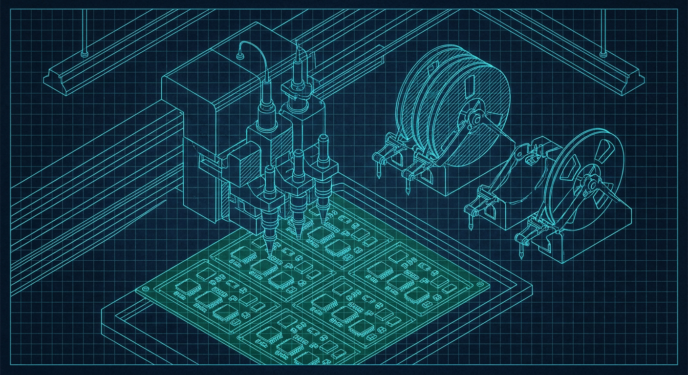
Contract manufacturers handling high-mix, low-volume (HMLV) electronics production have quietly updated their quoting algorithms over the past several quarters. Where fabrication and assembly shops once billed a flat line-item setup fee alongside a per-joint soldering charge, modern automated quoting engines now penalize bill-of-materials (BOM) fragmentation directly. If you submit a 200-piece run with eighty distinct part numbers, your tooling and setup line item will routinely eclipse the bare board fabrication and raw component costs combined.
For a solo hardware engineer or a small design team building industrial controllers, IoT gateways, or robotics compute modules, these hidden setup charges eat prototype budgets alive. You might spend three weeks tuning a schematic to perfection, carefully picking exact resistor values for every biasing network, only to discover that the assembly house charges a twenty-dollar feeder setup fee for each distinct component reel. When thirty of those reels contain resistors that differ by less than five percent in non-critical circuits, you are burning capital on factory idle time.
Understanding how high-mix SMT lines operate allows you to design boards that move through pick-and-place lines rapidly, eliminate manual feeder changeovers, and keep unit costs predictable on runs between fifty and five thousand units.
The Real Mechanics of Feeder Slot Economics
To understand why contract manufacturers charge steep setup fees for sprawling BOMs, look at the physical constraints of a modern pick-and-place platform. A typical mid-tier SMT placement system, such as a Juki, Yamaha, or Hanwha machine used on high-mix lines, houses between 80 and 120 eight-millimeter feeder slots. On an assembly line dedicated to high-volume consumer goods, these machines run untouched for weeks. On a high-mix line, an operator might retool the feeder bank three to six times per shift.
Retooling is not just snapping a tape into a slot. For every unique part number on your BOM, an assembly technician must retrieve the reel from moisture-controlled storage, verify the part number against the production traveler, mount the tape into an intelligent feeder, splice the tape leader if needed, calibrate the feeder pitch, and scan the barcode into the line management software. If your design calls for eighty unique line items, that setup sequence takes upwards of two hours of human labor before a single board enters the reflow oven.
When the job finishes running a batch of one hundred panels, the line stops. The operator tears down those reels, returns unused stock to inventory, and sets up the next customer's job. If your design uses 35 unique feeder slots instead of 80, the setup time drops by more than half. That difference directly determines whether your job fits into the standard queue or gets hit with an expedite penalty because it blocked a line for an entire morning.
+-----------------------------------------------------------------------------------+
|                         SMT LINE RETOOLING OVERHEAD                               |
|                                                                                   |
|  Fragmented BOM (85 Unique Parts):                                                |
|  [ Feeder Prep & Verification: 110 min ] --> [ SMT Run: 25 min ]                  |
|  Total Line Occupancy: 135 minutes (81% non-productive labor)                      |
|                                                                                   |
|  Rationalized BOM (32 Unique Parts):                                              |
|  [ Feeder Prep & Verification: 40 min ] --> [ SMT Run: 20 min ]                   |
|  Total Line Occupancy: 60 minutes (66% reduction in setup overhead)               |
+-----------------------------------------------------------------------------------+
Beyond labor, feeder capacity dictates machine pass counts. If your board requires 110 unique SMT components and the shop's primary placement machine only supports 90 feeder inputs, the factory must either run the panels through two sequential pick-and-place machines or execute a mid-run feeder swap. Both options double the risk of placement errors, increase cycle times, and introduce significant setup surcharges.
Passive Rationalization Across the Schematic
Passive components represent roughly 70 to 80 percent of the component count on a typical digital or mixed-signal PCB, yet they generate most of the unnecessary BOM complexity. Engineers frequently let their CAD tool inherit arbitrary resistor and capacitor values from application notes, reference designs, and simulation files.
A single board might contain 1.0k, 1.2k, 2.2k, 4.7k, 5.1k, and 10k ohm pull-up resistors across various communication buses and enable pins. In reality, nearly all digital pull-ups, pull-downs, and status LED current limiters can operate across a wide tolerance band without degrading circuit performance.
+-----------------------------------------------------------------------------------+
|                      PASSIVE CONSOLIDATION FRAMEWORK                              |
|                                                                                   |
|  Raw Schematic Values               Consolidated Standard Part                    |
|  --------------------               --------------------------                    |
|  1.0k (I2C Standard Speed)
|  1.5k (USB D+ Pullup)        -----> 2.2k 0402 1% (Covers I2C, general straps)     |
|  4.7k (I2C Fast Mode)        -----> 4.7k 0402 1% (Standardized bus pull-up)       |
|  10k (MCU Pin Straps)        -----> 10k  0402 1% (Standardized logic pull-up)     |
|                                                                                   |
|  10nF (ADC Filter)                                                                |
|  47nF (PLL Bypass)           -----> 100nF 0402 16V X7R (Universal Decoupling)     |
|  100nF (Digital VDD Bypass)                                                       |
|                                                                                   |
|  1.0uF (LDO Output)                                                               |
|  2.2uF (Buck In)             -----> 4.7uF 0603 25V X5R (Standardized Local Bulk) |
+-----------------------------------------------------------------------------------+
Digital Logic and Communication Strapping
Most microcontroller, FPGA, and SoC general-purpose input/output (GPIO) pins require pull-up or pull-down resistors between 1k and 100k ohms. Unless you are dealing with high-speed open-drain buses with tight rise-time requirements, standardizing on exactly two resistor values for all digital logic pins simplifies procurement.
Standardize on 10k ohm 1 percent resistors for static configuration pins, active-low reset lines, and chip enables. Use 2.2k or 4.7k ohm resistors for I2C and SMBus lines. Eliminate 1.5k, 3.3k, and 5.1k ohm parts unless an interface specification explicitly demands an exact impedance match, such as USB full-speed termination or Ethernet magnetic termination.
Decoupling and Bypass Capacitors
Decoupling networks are another major source of feeder bloat. Silicon vendor reference designs often specify a patchwork of 10nF, 47nF, 100nF, and 1.0uF ceramic capacitors placed in parallel across supply rails. Decades ago, combining staggered values was necessary to broaden the low-impedance bandwidth of through-hole or large-package capacitors with high equivalent series inductance (ESL).
Modern surface-mount multilayer ceramic capacitors (MLCCs) in 0402 and 0201 packages exhibit negligible package inductance. The mounting inductance introduced by vias and board traces dominates the impedance profile far more than the nominal capacitance value. In almost every case below 500 MHz, placing multiple identical 100nF (0.1uF) 0402 X7R capacitors provides equivalent or superior power distribution network (PDN) performance compared to a mixed assortment of 10nF and 100nF parts.
For local bulk storage on intermediate rails, standardize on a single 10uF 0603 or 22uF 0805 capacitor rated for at least twice your operating voltage to account for DC bias degradation. Avoid populating intermediate values like 2.2uF or 4.7uF unless physical height constraints prevent standardizing on the larger capacitance.
LED Current-Limiting Resistors
Status indicators and diagnostic LEDs often end up with half a dozen unique ballast resistor values because an engineer calculated the exact series drop for red, green, blue, and amber diodes to hit identical milliamp targets. On modern high-efficiency LEDs, human eyes perceive changes in luminous intensity logarithmically. Standardizing on a single 1.0k or 470 ohm resistor across all indicator colors rarely produces an objectionable visual difference, yet it eliminates three to four distinct reels from the machine feeder bank.
Standardizing Passive Footprints for SMT Yield
BOM consolidation is not just about electrical values. It is equally about footprint geometry. Placing five different package sizes of the same component value forces nozzle changes on the pick-and-place head, slows machine placement rates, and complicates optical inspection.
On low-to-medium volume production runs, the sweet spot for passive components is the 0402 (1005 metric) footprint. Components in the 0402 package are small enough to enable dense routing under tight microcontrollers and high-density ICs, yet large enough that standard high-mix pick-and-place machines can mount them at full rated speed without requiring specialized ultra-fine-pitch vacuum nozzles. They also exhibit significantly higher mechanical reliability and lower tombstoning rates in standard reflow ovens than 0201 or 01005 packages.
+---------------------------------------------------------------------------------+
|                       PACKAGE SELECTION TRADE-OFF MATRIX                        |
|                                                                                 |
| Package | High-Mix SMT Feasibility | Hand Rework | Feeder Space | Typical Use   |
| ------- | ------------------------ | ----------- | ------------ | ------------- |
| 0201    | Poor (Special Nozzles)   | Extreme     | High Density | Smartwatches  |
| 0402    | Excellent                | Moderate    | Optimal      | Default Pass. |
| 0603    | Excellent                | Easy        | Moderate     | High-V, Bulk  |
| 0805    | Excellent                | Very Easy   | Low Density  | Power Loops   |
+---------------------------------------------------------------------------------+
Reserve 0603 (1608 metric) packages for power rails where current demands exceed the thermal dissipation limit of an 0402 part, or where higher voltage ratings (such as 25V or 50V MLCCs) require thicker dielectric spacing. Avoid using 0805 or 1206 packages for common logic passives unless you require them for mechanical stand-off height or specialized pulse-handling capabilities.
When standardizing on 0402 passives, maintain consistent component spacing across the board. Automated optical inspection (AOI) systems and pick-and-place cameras identify parts faster and generate fewer false-positive placement faults when spacing between adjacent passive components is maintained at a minimum of 0.5 mm, with 0.8 mm between passive pads and adjacent IC leads.
Panelization, Tooling Strips, and Fiducial Geometry
For production runs under five thousand units, bare boards are rarely processed as individual circuits. They are panelized into arrays with breakaway tabs or V-score grooves. How you design this panel directly dictates whether the factory can run your job through automated optical inspection and high-speed placement or if they must slow the conveyor down.
+-----------------------------------------------------------------------------------+
|                         PANEL FIDUCIAL PLACEMENT RULES                            |
|                                                                                   |
|  +-----------------------------------------------------------------------------+  |
|  | (F1) Tooling Strip [5.0mm Clear Zone]                                       |  |
|  |  +-------------------------+     +-------------------------+                |  |
|  |  |                         |     |                         |                |  |
|  |  |   [Board 1]             |     |   [Board 2]             |                |  |
|  |  |                         |     |                         |                |  |
|  |  |           (f_local)     |     |           (f_local)     |                |  |
|  |  |           [QFN / BGA]   |     |           [QFN / BGA]   |                |  |
|  |  |                         |     |                         |                |  |
|  |  +-------------------------+     +-------------------------+                |  |
|  |                                                                        (F2) |  |
|  |  +-------------------------+     +-------------------------+                |  |
|  |  |                         |     |                         |                |  |
|  |  |   [Board 3]             |     |   [Board 4]             |                |  |
|  |  |                         |     |                         |                |  |
|  |  +-------------------------+     +-------------------------+                |  |
|  | (F3) Tooling Strip                                                          |  |
|  +-----------------------------------------------------------------------------+  |
|                                                                                   |
|  Key:                                                                             |
|  (F1, F2, F3) = Asymmetric Global Panel Fiducials (1.0mm copper / 2.0mm mask)     |
|  (f_local)    = Local Fine-Pitch Fiducials (Diagonal corners of QFN/BGA)          |
+-----------------------------------------------------------------------------------+
Global Panel Fiducials
A pick-and-place machine uses vision systems to align the physical board with the CAD centroid coordinates (X-Y pick-and-place file). To establish coordinate origin and compensate for thermal expansion or board flex, the panel must include global fiducials on the sacrificial tooling rails.
Place at least three global fiducials on the perimeter tooling strips. Crucially, position them asymmetrically. If an operator accidentally loads a panel backward or upside down into the conveyor track, an asymmetric fiducial layout prevents the machine from executing the placement program on an inverted board. If the fiducials are placed symmetrically at exact mirror coordinates, the optical vision system will register the fiducials, assume correct orientation, and fire the placement head into raw FR4 or across incorrect traces.
A standard global fiducial should feature a solid circular copper pad with a diameter of 1.0 mm, surrounded by a circular solder mask opening with a diameter of 2.0 mm. Keep the clear area around the fiducial completely free of silkscreen, copper pours, or traces. Nickel-gold (ENIG) or bare copper with organic solderability preservatives (OSP) provides the highest optical contrast for machine vision systems. Avoid placing fiducials directly over HASL (Hot Air Solder Leveling) finishes if possible, as uneven solder meniscus creates optical reflections that confuse camera centering routines.
Local Component Fiducials
Global panel fiducials compensate for overall board stretch and conveyor tilt, but they are insufficient for fine-pitch components such as 0.4 mm pitch QFNs, wafer-level chip-scale packages (WLCSPs), or fine-pitch BGAs. Local thermal variations across the panel during reflow or minute stretch during routing can shift pads by 50 to 100 microns across a standard 200 mm panel.
For any IC with a pin pitch of 0.5 mm or below, place two local fiducials diagonally at opposite corners of the package footprint. Local fiducials ensure that the placement head re-zeros its coordinate grid immediately before executing the high-precision drop, eliminating lead-to-pad misalignment that leads to solder bridging.
Tooling Strips and Edge Clearance
Conveyor belts on pick-and-place machines, reflow ovens, and automated optical inspection stations clamp the edges of the PCB panel as it travels down the line. Maintain a strict edge exclusion zone on your tooling strips. A minimum rail width of 5.0 mm on both top and bottom edges is standard across most EMS lines. Within this 5.0 mm strip, no components, test points, or copper traces on outer layers should be present.
If your design features edge-mounted connectors, micro-USB or USB-C jacks that overhang the PCB edge, or board-edge RF antennas, orient them toward the internal routed cutouts between panelized sub-boards rather than toward the conveyor clamping rails. An overhanging component that collides with a conveyor belt roller will jam the line, trigger an emergency stop, and likely damage both the connector and the feeder head.
The Financial Impact of BOM Rationalization
To quantify how component consolidation influences low-volume manufacturing costs, consider an illustrative composite based on standard North American and European turnkey assembly pricing for small industrial controller boards.
Setup and SMT Run Comparison
The following table illustrates a batch run of 250 four-layer industrial sensor interface boards. The baseline version uses an unconstrained BOM straight from initial schematic capture. The rationalized version represents the same electrical design after two hours of component value consolidation, footprint unification to 0402, and panel-level fiducial standardization.
| Production Parameter | Baseline Unoptimized BOM | Rationalized SMT BOM | Engineering Variance |
|---|---|---|---|
| Total Component Count (per board) | 142 | 138 | -4 components (redundancies eliminated) |
| Unique Line Items (BOM lines) | 78 unique parts | 34 unique parts | -56% unique part numbers |
| Feeder Loading and Setup Time | 115 minutes | 42 minutes | -63% factory setup duration |
| Machine Changeovers Required | 1 (exceeded 80-slot feeder bank) | 0 (fits standard single pass) | Eliminated secondary line setup |
| Line Setup Fee (Factory Invoice) | $1,560 ($20 / line item) | $680 ($20 / line item) | $880 direct cost reduction (56%) |
| Pick-and-Place Machine Placement Time | 4.2 hours total batch run | 3.1 hours total batch run | 26% faster line throughput |
| AOI False-Positive Fault Rate | 4.8% (mixed passive footprints) | 0.9% (standardized 0402/0603) | Significant reduction in manual rework |
| Total Assembly Cost per Unit (250 qty) | $18.40 | $12.10 | $6.30 saved per board (34% savings) |
Note: Metrics represent an illustrative composite model derived from typical turnkey high-mix EMS rate structures ($80-$120/hr line rate, $15-$25 per-feeder setup charge, 250-unit batch size).
The engineering time required to consolidate those values was approximately two hours during schematic capture. The resulting manufacturing savings totaled $1,575 on a single 250-piece run, while simultaneously reducing the risk of component obsolescence during future production reorders.
What This Means for IntelCAD
Designing for automated assembly requires layout environments that connect schematic intent with physical manufacturing reality. Modern design flows cannot treat component selection as an isolated exercise performed in a vacuum before routing begins.
IntelCAD incorporates physics-aware layout and live supply chain data directly into the design canvas. By evaluating component availability, package standardization, and pin clearance constraints alongside automated trace routing, the platform prevents the common trap of selecting obsolete or non-standard parts during early layout. Rather than relying on static design rule checks after layout completion, automated routing and placement tools must optimize for assembly efficiency, ensuring panel fiducials, component orientations, and passive footprints adhere to high-mix production standards from the first prototype spin.
Practical Checklist for Pre-CAM BOM Consolidation
Before you generate Gerber files, ODB++ packages, and centroid data for your next small-batch run, run your design through this pre-flight consolidation sequence:
+-----------------------------------------------------------------------------------+
|                      PRE-CAM BOM AUDIT CHECKLIST                                  |
|                                                                                   |
|  [ ] 1. Run BOM Value Histogram: Flag any resistor/capacitor used < 3 times.       |
|  [ ] 2. Standardize Logic Straps: Consolidate all digital pull-ups to 10k 0402.   |
|  [ ] 3. Merge Decoupling Caps: Replace single 10nF/47nF caps with 100nF 0402 X7R. |
|  [ ] 4. Unify LED Resistors: Standardize status LED ballasts to one single value.  |
|  [ ] 5. Audit Package Sizes: Confirm >80% of passives share the 0402 footprint.   |
|  [ ] 6. Inspect Panel Fiducials: Ensure 3 asymmetric fiducials on tooling rails.   |
|  [ ] 7. Place Local Fiducials: Verify diagonal fiducials on ICs with <0.5mm pitch.|
+-----------------------------------------------------------------------------------+
- Run a BOM Line-Item Histogram: Export your component list to a spreadsheet or database view. Sort by component quantity. Any passive component with a usage count of one or two should be scrutinized. Can that single 4.7k resistor be swapped for the 10k value used elsewhere on fifty pins? Can that isolated 22nF capacitor be replaced with your ubiquitous 100nF decoupling cap?
- Lock Down Voltage Ratings on MLCCs: When consolidating capacitors, ensure the unified part number carries a voltage rating suitable for the highest-voltage rail it touches. Standardizing on a 100nF 50V X7R 0402 capacitor allows you to use the exact same reel across 3.3V logic rails, 12V intermediate supplies, and 24V industrial inputs without risking dielectric breakdown or severe DC bias capacitance loss.
- Verify Component Orientations in the Centroid File: Ensure all polarized components (diodes, tantalum capacitors, ICs, polarized connectors) follow IPC-7351 standard zero-orientation rules in your footprint library. Mismatches between your CAD zero-degree definition and the EMS reel-tape orientation lead to inverted diode placements that must be reworked by hand after reflow.
- Confirm Panel Breakaway Clearance: Verify that no surface-mount component sits closer than 1.0 mm to a V-score cut line, or closer than 2.0 mm to a mouse-bite perforation tab. The mechanical stress of panel singulation can crack brittle ceramic MLCCs, causing intermittent short circuits that pass initial factory testing and fail weeks later in the field.
By treating the pick-and-place line as an integral part of your design constraints, you eliminate setup penalties, cut factory turnaround times, and ensure that your small-batch production runs remain economically viable.